
The Ultimate PCB Design Guide for Manufacturing Success
1. Introduction: The Essential PCB Design Guide for Manufacturing Success
This PCB design guide delivers the essential principles required to transition your digital layout into a flawless physical reality. When embarking on a new project, engineers often expend the bulk of their time on circuit design and component selection, leaving the layout and routing phases vulnerable to costly manufacturing defects or functional failures due to a lack of comprehensive planning. The definitive answer to building a reliable board lies in designing for manufacturability (DFM) from the start, which requires meticulously managing component placement, enforcing strategic routing, and executing rigorous thermal dynamics controls.
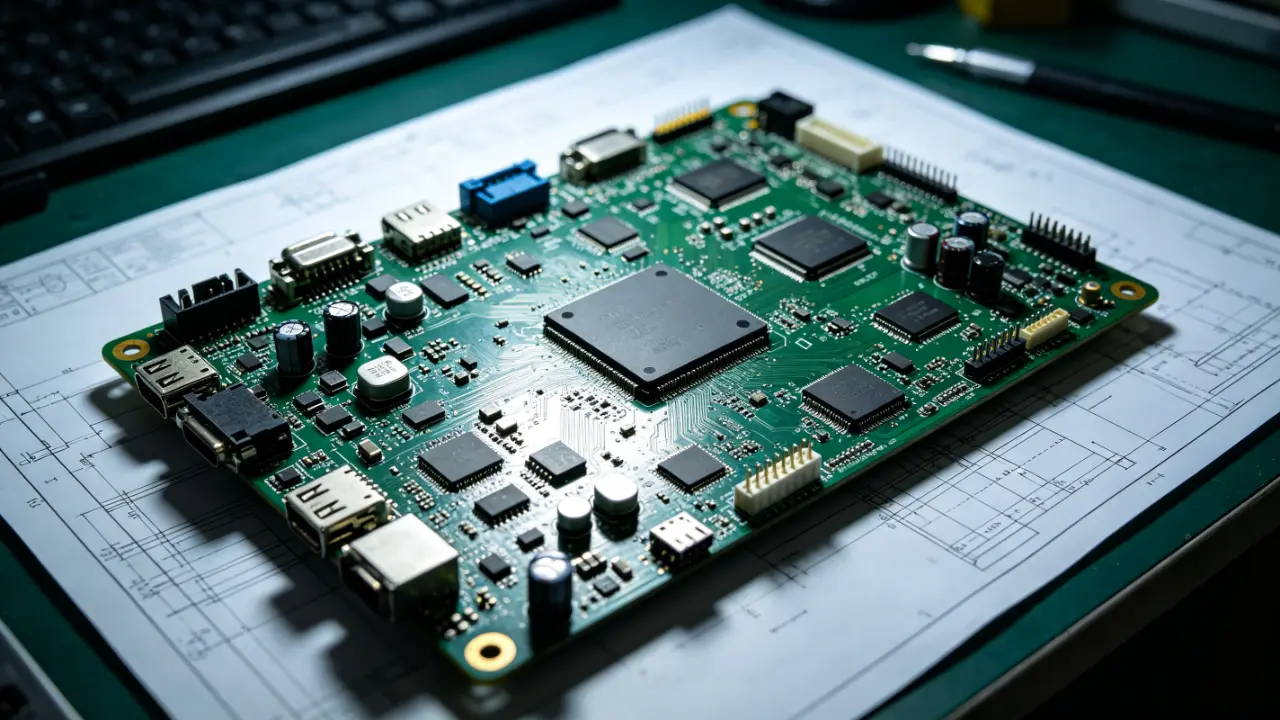
As a direct factory manufacturer operating without middlemen, we see firsthand how layouts optimized for advanced PCB design manufacturing lines lower assembly costs and accelerate time-to-market. We provide deep technical feedback directly from the assembly floor to ensure your boards perform exactly as intended, bridging the gap between theoretical schematics and robust electronic manufacturing services.
Key Takeaways:
- Strategic Component Placement: Orient and organize components to streamline assembly steps and minimize physical interference during soldering.
- Robust Signal & Power Routing: Utilize internal plane layers and optimized trace widths to maintain signal integrity and board structural stability.
- Advanced Thermal Management: Implement thermal relief pads to prevent reflow anomalies like cold joints or de-wetting on massive copper pours.
- Pre-Manufacturing Validation: Execute strict Electrical Rule Checks (ERC) and Design Rule Checks (DRC) prior to final fabrication.
2. Fine-Tuning Component Placement for Manufacturability
The placement phase is both a science and an art, demanding strategic calculation regarding the available primary components to ensure the board is easily manufacturable and meets your baseline design requirements. The physical coordinates and alignment of your parts directly dictate the efficiency and yield rate of the factory floor.

2.1 Orientation and Arrangement Protocols
- Consistent Component Orientation: Aligning similar components in identical directions is a fundamental guideline that helps facilitate a highly efficient and error-free soldering process.
- Shadowing Prevention in Arrangement: It is crucial to avoid placing smaller components directly behind larger ones. Larger component bodies can disrupt the thermal profile or solder wave, creating physical mounting issues for the smaller shielded parts.
2.2 Organizing Surface Mount and Through-Hole Technologies
- Layer Segregation: To optimize contract PCB assembly, group all Surface Mount Technology (SMT) components on a single side of the board and restrict all Through-Hole (TH) components to the top side, which minimizes redundant assembly steps.
- Mixed Technology Cost Implications: Utilizing a hybrid approach with both TH and SMT assembly parts means the manufacturer will likely require additional processing steps to assemble the circuit board, directly increasing your overall production costs.
3. Strategic Routing for Power, Ground, and Signal Integrity
Once your components are physically locked in, establishing clean, interference-free pathways for power, ground, and signals is the next critical engineering phase.

3.1 Structuring Power and Ground Planes
- Symmetrical Internal Planes: Power and ground planes should be localized to the internal layers of a multilayer PCB while remaining symmetrical and centered. This structural balance helps prevent board warpage during high-temperature manufacturing, ensuring your components remain correctly seated.
- Direct IC Power Delivery: For supplying power to Integrated Circuits (ICs), utilize common channels with robust and stable trace widths. Engineers must strictly avoid daisy-chained power connections from component to component.
3.2 Signal Trace Routing and Exit Strategies
- Shortest Path Optimization: Always route signal lines following the shortest and most direct path between components based on the schematic’s logic.
- Horizontal Exit to Prevent Skewing: When components must maintain a strict horizontal orientation without deviation, design traces to exit the component horizontally before transitioning to a vertical route. This prevents solder migration and fluid dynamics during reflow from physically skewing the component off its axis.
- Current-Dependent Trace Widths: Low-current analog and digital signals typically require a baseline 0.010″ (10 mil) network width constraint. Traces carrying currents exceeding 0.3 Amperes demand proportional widening to handle the load safely.
3.3 Electrical Isolation and Coupling Mitigation
- Ground Separation in 4-Layer Stacks: Whether utilizing standard dual-layer or 4-layer PCB fabrication, maintain strict isolation between power ground and control ground networks to prevent high-voltage spikes from disrupting low-voltage circuits. If they must merge on the board, tie them together as close to the terminus of the power path as possible.
- Impedance Control: When utilizing a mid-layer ground plane, design a low-impedance path to reduce interference risks from power circuits and safeguard control signals.
- Capacitive Coupling Reduction: To minimize coupling effects caused by routing above and below massive ground planes, ensure that only analog signal lines intersect the analog ground plane.
4. Advanced Thermal Management Techniques
Thermal dynamics play an immense role in board longevity and performance. Have you ever experienced component degradation or catastrophic board failure simply because heat dissipation was an afterthought? Resolving thermal accumulation is not a feature; it is an absolute baseline requirement for reliable hardware.

4.1 Identifying and Mitigating Heat Sources
The primary objective is to pinpoint exactly which silicon packages or discrete components will dissipate the most thermal energy under maximum load. Properly selecting PCB materials with favorable thermal conductivity can establish a strong foundation, but layout strategy remains paramount.
- Thermal Resistance Evaluation: To map your board’s thermal profile, engineers must first consult component datasheets to locate the exact “thermal resistance” ($\theta_{JA}$ or $\theta_{JC}$) ratings. This metric dictates how efficiently a package transfers internal junction heat to the ambient environment.
- Active and Passive Dissipation Planning: Once high-heat components are identified, integrate physical mitigation strategies such as appropriately sized heat sinks and active cooling fans to aggressively pull temperatures down.
- Strategic Thermal Isolation: A critical rule of placement is to isolate sensitive, high-precision control circuits by keeping them physically distant from any primary high-heat sources like power MOSFETs or regulators. Upgrading to high Tg FR4 PCBs provides a wider operating margin, but physical separation remains the most effective defense against localized thermal runaway.
5. The Critical Role of Thermal Relief Pads in Soldering
Process engineers operating Surface Mount Technology (SMT) lines frequently encounter persistent manufacturing defects such as solder empty, de-wetting, or cold solder joints. While component oxidation is sometimes to blame, root-cause analysis routinely traces these faults directly back to flawed layout practices—specifically, the direct connection of component pins to massive copper pours without proper thermal restriction.
5.1 Understanding Solder Defects on Massive Copper Pours
Power (Vcc, Vdd) and ground (GND) networks often utilize large area copper foils connected directly to the pins of control ICs and discrete components. These massive copper planes act as massive, highly efficient heat sinks.
- Asymmetrical Heating Profiles: When attempting to heat these massive copper areas to the solder melting point, they demand significantly more time and thermal energy compared to isolated pads, while simultaneously dissipating that heat much faster.
- The Solder Imbalance: When a trace connects a small resistor or capacitor to a massive copper pour on one end, but a standard pad on the other, the mismatched melting and solidification times inevitably trigger severe soldering defects.
- Reflow and Manual Soldering Failures: If the reflow profile lacks adequate preheating, pins tied directly to copper planes fail to reach the necessary wetting temperature, yielding cold or false joints. During manual soldering, rapid heat dissipation prevents the technician from forming a proper joint within a safe timeframe, often causing them to dangerously increase iron temperatures—risking permanent component destruction.
5.2 Engineering Thermal Relief Geometries
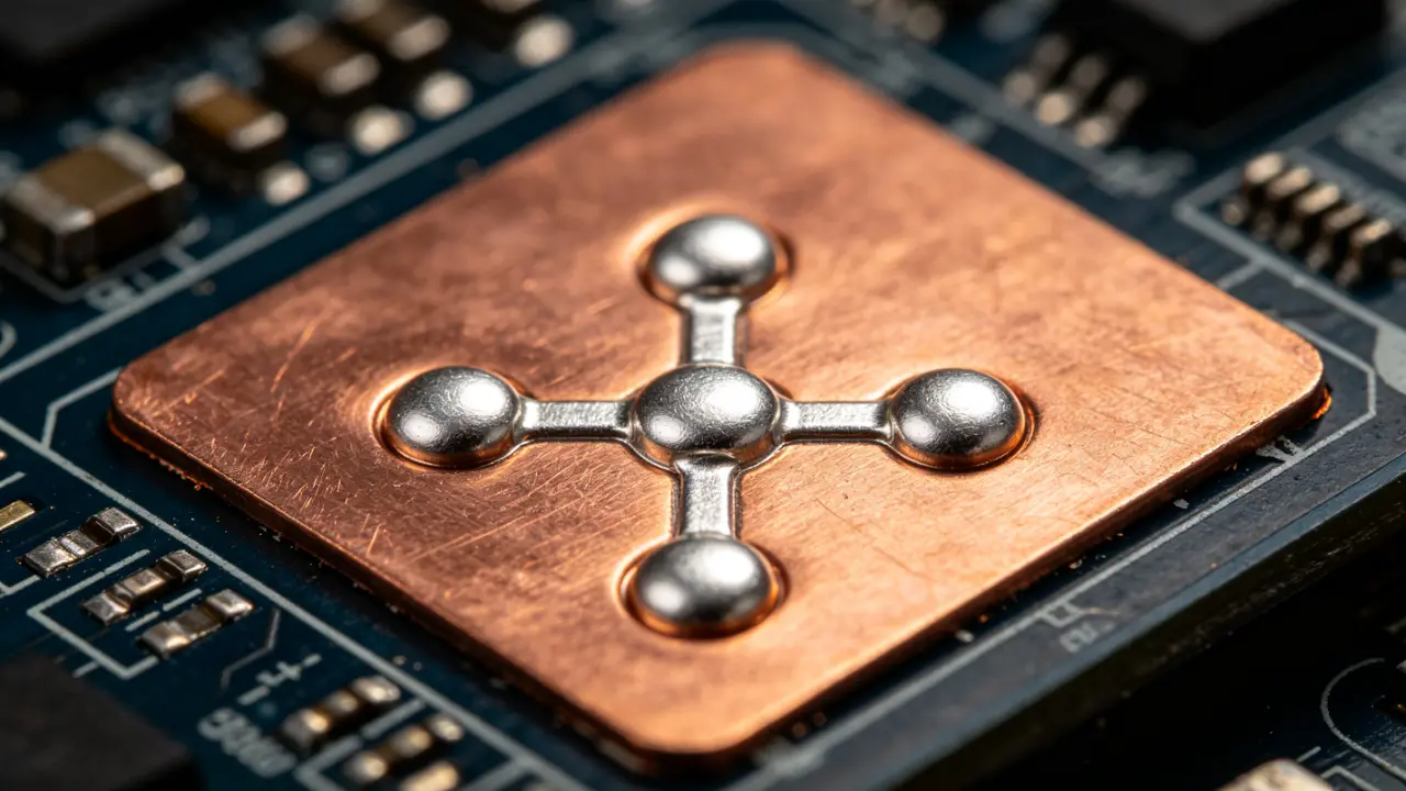
The industry-standard solution to this thermodynamic bottleneck is the implementation of thermal relief pads. Mastering PCB pad design ensures predictable solder dynamics across both automated and manual assembly.
- Spoke and Web Architectures: A thermal relief pad modifies the connection by limiting the contact area between the pad and the large copper foil to just a few narrow traces (spokes).
- Restricted Heat Flow: By physically necking down the copper connection, the thermal relief drastically limits the rate of heat loss from the pad during reflow, achieving highly optimal and consistent soldering results.
6. Pre-Manufacturing Validation: ERC, DRC, and Final Checks
When you are rushing to combine all circuit blocks for final manufacturing, it is dangerously easy to overlook critical layout errors that surface only after fabrication. Double and triple-checking your final design database at this exact stage is often the deciding factor between a successful prototype and a costly scrap run.

6.1 Automated and Manual Design Verification
Executing rigorous quality checks ensures the transition to PCB quality control at the factory goes smoothly without costly on-the-fly engineering holds.
- Automated Rule Enforcement: We heavily recommend running your software’s Electrical Rule Check (ERC) and Design Rule Check (DRC) to unequivocally verify that the layout strictly adheres to all defined constraints and rules.
- Parameter Verification: These automated systems rapidly scan for violations in trace widths, physical clearance, high-speed routing constraints, and dangerous short circuits.
- Manual Signal Tracing: Once the ERC and DRC yield a clean, zero-error report, you must still manually inspect the routing of individual signals. Trace each signal directly from the schematic to the physical layout one by one to ensure zero data was omitted.
- Tool Utilization: Leverage your CAD software’s probing and shielding features to cross-reference and confirm that your physical layout perfectly matches the original logical schematic.
6.2 Standard Verification Parameters
| Verification Type | Target Parameters | Factory Impact if Ignored |
| Electrical Rule Check (ERC) | Open circuits, short circuits, floating pins, logic conflicts | Total functional failure, immediate board rejection during flying probe testing. |
| Design Rule Check (DRC) | Trace clearances, via sizing, annular rings, silk-to-pad spacing | Unmanufacturable boards, solder bridging during wave/reflow. |
| Netlist Comparison | IPC-D-356 netlist vs. Gerber data mismatch | Assembly of functionally dead boards; high rework costs. |
7. Conclusion: Transitioning from Design to Factory-Direct Production
Mastering this PCB design guide means fundamentally shifting your perspective from purely logical circuit creation to physical manufacturing realization. By strategically orienting your components, carefully balancing your power and ground planes, implementing critical thermal relief structures, and executing rigorous DRC validations, you effectively eliminate the friction between digital intent and factory floor reality. These targeted DFM practices establish a baseline of continuous improvement, drastically reducing revision cycles and overall production costs.

When your verified design is ready for fabrication, partnering directly with the manufacturing floor removes costly middlemen and accelerates your time to market. Finest PCB provides unparalleled, one-stop electronic component assembly, leveraging decades of factory-direct expertise to build your boards exactly as engineered. Contact our engineering team today for a rapid, comprehensive quote and experience true manufacturing precision.
Frequently Asked Questions (FAQ)
What is the standard trace width for low-current signal routing? For low-current digital and analog signals, a baseline trace width of 0.010 inches (10 mils) is standard industry practice. However, if the network carries currents exceeding 0.3 Amperes, the trace must be proportionally widened to handle the thermal and electrical load.
Why do large copper planes cause cold solder joints? Large, unbroken areas of copper act as massive heat sinks during the reflow process. They pull thermal energy away from component pins faster than standard pads, preventing the solder from reaching its proper wetting temperature and resulting in defective, cold solder joints.
What is the difference between ERC and DRC? Electrical Rule Checks (ERC) verify the logical functionality of the schematic, ensuring no conflicting outputs, floating inputs, or logic errors exist. Design Rule Checks (DRC) validate the physical layout against the manufacturer’s capabilities, checking spatial parameters like trace clearances, via drill sizes, and board edge spacing.
Should surface mount and through-hole components be placed on the same side? To minimize manufacturing steps and lower assembly costs, engineers should group all Surface Mount Technology (SMT) components on one side of the board and place all Through-Hole (TH) components on the top side. Mixing them haphazardly requires complex, multi-stage soldering processes.