
FR4 PCB General Capabilities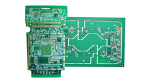
Definition and explanation of FR4 PCBs.
FR4 material is a PCB substrate that comes in the form of epoxy-reinforced glass fiber laminates. Due to its rugged nature and flame retardant properties, it is a common laminated substrate in printed circuit boards. Therefore, it is essential to provide the required insulation for the board. FR4 PCBs, an essential cornerstone of the PCB manufacturing process, refer to Printed Circuit Boards that are crafted using a composite material known as FR4. This material’s acronym originates from “Flame Retardant 4,” highlighting its remarkable resistance to combustion and its role in enhancing safety in the realm of PCB manufacturing process.
In the intricate landscape of PCB manufacturing, FR4 material serve as the very canvas upon which the intricate tapestry of electronic components is meticulously woven. They provide the structural foundation necessary to support, interconnect, and power the various components that collectively breathe life into an extensive array of electronic devices. These circuit boards play a pivotal role in connecting and powering electronic components, ensuring the seamless functioning of countless devices that define our digital age.
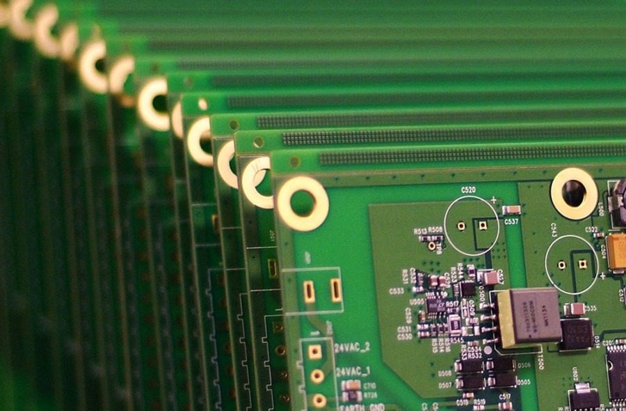
The composition of FR4 material is a well-engineered blend of materials that combine to offer the desired electrical, thermal, and mechanical characteristics. At its core is an epoxy resin matrix infused with woven fiberglass. This combination grants the PCB its rigidity and strength, allowing it to withstand the demands of various applications. Copper foil layers are bonded to the substrate, creating conductive pathways that enable the flow of electrical signals.
At its core lies an epoxy resin matrix seamlessly interwoven with layers of fiberglass. This marriage of materials results in a substrate that boasts impressive mechanical durability, perfectly suited for the exacting demands of the PCB manufacturing
Properties of FR4 PCBs
FR4 material PCBs, integral to the world of PCB manufacturing, boast a spectrum of properties that make them a sought-after choice in electronic design. As an essential constituent of the PCB manufacturing materials landscape, FR4 offers a unique blend of attributes that contribute to its widespread use, cost-effectiveness, and versatility.
Electrical Properties:
FR-4 exhibit consistent electrical characteristics, making them well-suited for a range of applications. Their dielectric constant and loss tangent facilitate effective signal propagation, a critical factor in high-frequency circuits. This makes FR-4 PCBs valuable in industries that demand reliable data transmission and communication.
Thermal Properties:
While not the most thermally conductive material, FR-4 PCBs effectively manage heat generated by electronic components during the PCB manufacturing process. Their ability to dissipate heat helps maintain the stability of circuits and prevents performance degradation due to excessive temperatures.
FR-4 exceptional tensile and flexural strength lend them durability, ensuring they can withstand the rigors of handling, assembly, and operation. This resilience extends the lifespan of devices and contributes to their reliability, a paramount consideration in the PCB manufacturing process.
Chemical Resistance:
FR-4 PCBs exhibit resistance to chemicals, solvents, and moisture, a vital characteristic for maintaining performance and reliability over time. This property safeguards devices against environmental factors and contributes to their longevity.
Balancing PCB Manufacturing Costs:
FR-4 PCBs are favored not only for their technical attributes but also for their cost-effectiveness. In the realm of PCB manufacturing costs, the availability and wide use of FR4 materials contribute to their affordability. Their balanced combination of performance and price point makes them an attractive choice, especially for applications where optimizing PCB manufacturing price is crucial.
The general technical indicators of FR-4 sheet material are: bending strength, peeling strength, thermal shock performance, flame retardant performance, volume resistance coefficient, surface resistance, dielectric constant, dielectric loss Angle tangent, glass transition temperature Tg, dimensional stability, maximum service temperature, warpage degree, etc.
Dielectric Constant and Loss Tangent
FR4’s dielectric properties influence signal propagation and integrity, making it suitable for high-frequency applications.
Glass Transition Temperature (Tg)
FR4 maintains its mechanical strength and stability even at elevated temperatures, ensuring reliability in demanding conditions. The most obvious difference between FR-4 materials is the Tg value, according to the Tg temperature, FR-4 plates are generally divided into low Tg, medium Tg and high Tg plates. In the industry, FR-4 Tg of about 135℃ is usually classified as low Tg sheet; The FR-4 of Tg at about 150℃ is medium Tg plate; FR-4 Tg at about 170℃ is classified as high Tg plate.
If the PCB is processed with more times of pressing, or more PCB layers (more than 14 layers), or the welding temperature is high (≥230℃), or the working temperature is high (more than 100C), or the welding thermal stress is large (such as wave welding), high Tg plate should be selected.
Tensile and Flexural Strength
FR4’s robust mechanical properties offer resistance against bending, impact, and other stresses.
Applications of FR4 PCBs
As a cornerstone of modern electronics, find themselves at the heart of a diverse range of applications. Their versatile nature, compatibility with Multilayer PCB designs, and integral role in the PCB manufacturing process have solidified their position across various industries, from consumer electronics to cutting-edge technology. They had applicated in many different electronic area.
Consumer Electronics PCB: FR4 are the unsung heroes within our gadgets. In smartphones, tablets, and laptops, they enable seamless connectivity, data processing, and power distribution. As Multilayer PCB designs become increasingly prevalent, FR4 material accommodate the intricate circuitry required by these devices. The integration of various components within compact spaces is a testament to their efficiency.
Industrial Control PCB: In the realm of industrial automation, it play a pivotal role in control systems, robotics, and factory automation. These applications demand precision and reliability, both of them deliver. Their mechanical stability, resistance to environmental factors, and adaptability to the complexities of PCB manufacturing automation make them a cornerstone of industrial progress.
Automotive PCB: Contribute to the advancement of automotive technology. They power engine control units (ECUs), infotainment systems, safety features, and navigation systems. The intricate Multi-Layer PCBs in these applications necessitate a material that can facilitate the complex interconnections required for modern vehicles.
Telecommunications PCB: Routers, switches, and communication devices rely on High performanc PCBs to maintain connectivity in the digital age. These intricate networks demand high-performance Multilayer PCBs to ensure data transmission efficiency and reliability. FR4’s properties enable the construction of robust and dependable communication systems.
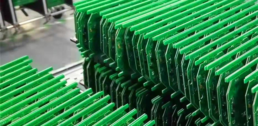
PCB Assembly Service and Rapid Prototyping: FR4 play a crucial role in the PCB assembly service landscape. Their compatibility with automated assembly processes streamlines production, ensuring efficient and cost-effective manufacturing. Moreover, in PCB rapid prototyping, FR4 enable designers to iterate and refine their designs swiftly, allowing for faster time-to-market for new products.
As technology evolves, the applications of Advanced PCB manufacturing continue to expand. Their role in Multilayer PCB designs, coupled with their contribution to PCB manufacturing automation and rapid prototyping, positions them as an indispensable asset in the realm of modern electronics.
FINEST Pinted Circuit Board Ltd is a subsidiary of FINEST Group. It was established on April 2019, specializing in EMS Processing, SMT quick-turn prototype and small batch production. Finest PCBA team with the ability to selecting materials, making samples and small batch production, and donging testing services. We always improve research and development efficiency, aiming at providing fast service to satisfies customers’ different demands for PCB assembly. Free to send us your file for quote, we ill resonse you within 24 hours.
- Single Sided PCB
- Double Sided PCB
- Multi-Layer PCB
- Buried Via PCB
- Blind Via PCB
- Impedance Controlled PCB
- Micro Via PCB
- Laser Drilling PCB
- RoHS Compliance PCB
- Epoxy filled vias PCB
FR4 PCB Specific Capabilities
|
Attribute: see (*) below as applies |
S/Sided |
D/Sided |
Multilayer |
Advanced |
|
Minimum Line/Spacing, Internal Layer |
N/A |
N/A |
.004”/.004” |
.003”/.003” |
|
Minimum Line/Spacing, External Layer |
.007”/.008” |
.007”/.008” |
.005”/.005” |
.003”/.003” |
|
Aspect Ratio (Thickness to Drill) |
6:1 |
6:1 |
8:1 |
10:1 |
|
Minimum Drilled Hole Size |
.010” |
.008” |
.008” |
.008” |
|
Land Size Internal (Diameter Over Drill) |
N/A |
N/A |
.015” |
.012” |
|
Land size External (Diameter Over Drill) |
.012” |
.012” |
.012” |
.010” |
|
Plane Clearance (Diameter Over Drill) |
.030” |
.030” |
.030” |
.024” |
|
Plated Hole Tolerance |
+/- .003” |
+/- .003” |
+/- .003” |
+/- .002” |
|
Minimum Dielectric Thickness |
N/A |
N/A |
.0025” |
.002” |
|
Minimum Core Thickness |
N/A |
N/A |
.004” |
.003” |
|
Minimum PCB Thickness ** |
.017” |
.018” |
.020” |
.020” |
|
Maximum PCB Thickness |
.125” |
.125” |
.250” |
.250” |
|
Thickness Tolerance (%) |
+/- 10 |
+/- 10 |
+/- 10 |
+/- 5 |
|
Maximum Board Dimensions * |
16” x 52”* |
19” x 22”* |
17” x 23”* |
17” x 23”* |
|
Fabrication Tolerances (overall dimension) |
+/- .010” |
+/- .010” |
+/- .010” |
+/- .005” |
|
Bow and Twist (Through Hole) % |
1.5 |
1.5 |
1.5 |
1 |
|
Bow and Twist (SMT) % |
.75 |
.75 |
.75 |
.75 |
|
Minimum Conductor to Edge |
.015” |
.015” |
.015” |
.010” |
|
Layer to Layer Registration Tolerance |
N/A |
.004” |
.004” |
.003” |
|
Component Pitch |
.025” |
.025” |
.025” |
.015” |
|
Soldermask Clearance |
.005” |
.005” |
.005” |
.004” |
|
Soldermask Dams |
.005” |
.005” |
.005” |
.004” |
|
Impedance Tolerance (>50 Ohms) % |
+/- 10 |
+/- 10 |
+/- 10 |
+/- 8 |
|
Maximum Layers |
1 |
1 |
12 |
16 |
|
Minimum Copper Weight Inners (oz.) |
N/A |
N/A |
|
1/4 |
|
Maximum Copper Weight Int. Ground (oz.) |
N/A |
N/A |
3 |
8 |
|
Maximum Copper Weight Int. Signal (oz.) |
N/A |
N/A |
2 |
6 |
|
Maximum Copper Weight Ext. Ground (oz.) |
4 |
4 |
2 |
10 |
|
Maximum Copper Weight Ext. Signal (oz.) |
4 |
4 |
3 |
10 |