Precision Crafted Custom PCBs Tailoring Circuit Solutions
Embark on a journey through the intricate landscape of bespoke Custom PCBs design, where each choice in material and method is a deliberate stroke of genius. Here, at Finest Printed Circuit Board Ltd, we don’t just assemble; we sculpt the very conduits of innovation, one custom circuit at a time. Delve with us into the meticulous world where personalized design weds state-of-the-art technology, and discover how our tailored PCBs are the silent yet potent heartbeat of industry advancements.
1. Introduction to Custom PCBs
In the electric hum of circuitry innovation, ‘PCB’ might suggest a certain sameness, but that’s a façade. True progress is handcrafted, piece by piece. At the heart of every technological leap is a custom circuit board, which I shape with care to meet its singular destiny. It’s in these unique creations that the magic of a custom solution shines, offering a level of detail the standard options just can’t touch.
The Genesis of Tailored Circuit Solutions
Crafting a custom circuit board is much like a master tailor pouring over the creation of a bespoke suit. It all starts with a deep dive into its intended purpose. Just as a tailor selects just the right fabric and cut to complement the wearer, I design each circuit board with the device’s unique needs in mind. My approach to design is far from just ticking boxes; it’s about going above and beyond. I ensure that every board I create isn’t just another part—it’s the foundation of a technological work of art.
Beyond the One-Size-Fits-All Approach
Eschewing the archaic notion that a singular approach suffices, I delve into the essence of these bespoke circuit panels. Their true narrative unfolds not merely in their assembly but in the opportunities they engender. Our discourse transcends mere construction, venturing into the realm of ingenuity they spark within our daily digital companions. Consider the ingenious orchestration of components that augments the end-user’s interaction, the astute thermal governance that escalates a gadget’s power thriftiness, and the harmonious fusion of a board’s resilience with its aesthetic. It is this marriage of elegance and utility that captivates my interest.
The Unseen Artistry in Electronics
In a realm dominated by the uniformity of mass fabrication, the nuanced artisanship in forging these singular circuitry solutions frequently escapes notice. Nevertheless, it is precisely this artisanal touch that elevates a utilitarian apparatus to a remarkable one. It’s about recognizing that the worth of these boards transcends mere connectivity of electronic elements; it lies in their potential to transform a concept into a tangible reality.
The Pinnacle of Personalization
Venturing further into the electronics domain, we discover that the zenith of circuit board craftsmanship extends beyond mere customization. It’s about attaining an exquisite equilibrium between aesthetics and utility. This is the realm where engineers and designers, akin to modern-day alchemists, transmute mundane materials into vessels of ingenuity. Here, the journey diverges from simple production to the sculpting of a legacy — each circuit a testament to this enduring pursuit.
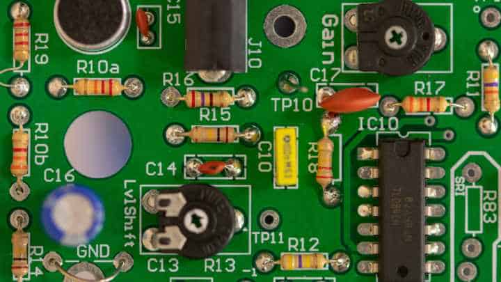
2. Understanding PCBs and Their Importance
Printed Circuit Boards (PCBs) stand as the unsung foundation of the electronics sector, their pivotal function frequently eclipsed by the more glamorous elements they underpin. Far from just passive substrates, these boards constitute the fundamental groundwork that anchors every advancement in the realm of electronics.
The Heart of Modern Electronics
Envision each electronic gadget as a thriving metropolis. Within this metaphor, PCBs are akin to the essential infrastructure — the thoroughfares and viaducts — facilitating the movement of electronic currents. Absent these critical pathways, electrical components would remain isolated, leaving the devices inert.
- Conduits of Interaction: PCBs lay down the intricate network of routes for electricity and signals to traverse among diverse elements.
- Structural Sustenance: These boards offer a sturdy scaffold for various constituents like resistors, capacitors, and microchips.
- Thermal Regulation: PCBs serve to channel heat away from vital components, safeguarding the device’s operation within optimal thermal thresholds.
The Evolution of PCB Complexity
The intricacy of PCBs has undergone considerable advancement. Initial iterations were straightforward, featuring a solitary layer. Contemporary designs, however, boast numerous strata — with some encompassing a dozen or more — each layer contributing to the enhanced functionality and condensed form of the end product.
- Single-Layer Boards: Employed within basic electronic devices such as calculators.
- Multi-Layer Boards: Integral to complex apparatuses such as smartphones and laptops.
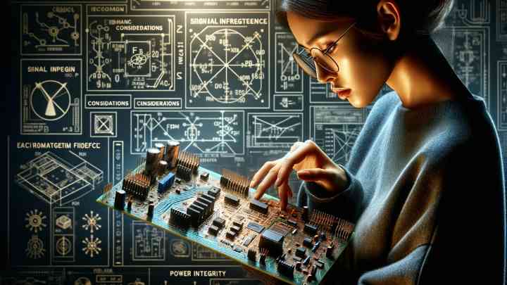
The Unseen Challenges in PCB Design
Rarely broached is the delicate interplay of physics and engineering ingenuity infused into the design of PCBs. Crafters of these boards must navigate the complexities of electromagnetic interference (EMI), alongside maintaining the fidelity of signal and power integrity. These elements are paramount for the PCB’s dependable performance across varying operational scenarios.
- EMI Considerations: Pathways are meticulously architected to curtail interference that could compromise functionality.
- Signal Integrity: This involves the assurance that signals are conveyed with scant loss and distortion.
- Power Integrity: This pertains to the sustenance of consistent and uncontaminated power distribution across the circuit board.

The Material Matters
The selection of the substrate material is a critical determinant of a PCB’s efficacy. FR4 reigns as the conventional choice, yet alternatives such as Polyimide are employed in high-temperature contexts, and Rogers materials are favored for their proficiency in high-frequency applications.
- FR4 PCB Material: This ubiquitous substrate is celebrated for its equilibrium of affordability and performance, making it the go-to for a multitude of PCBs.
- Polyimide: Esteemed for its resilience to elevated temperatures, this material is indispensable in sectors like aerospace and automotive engineering.
- Rogers Material: Esteemed for its minimal dielectric loss, this substrate is essential for the integrity of high-frequency electronic circuits.
3. The Advantages of Custom PCBs
The era of a universal standard for embedding circuit boards into products has become antiquated. Tailor-made PCBs represent more than mere extravagance; they are a judicious allocation of resources. These bespoke boards provide subtle yet significant benefits that off-the-shelf PCBs cannot rival, particularly in aspects of performance, seamless integration, and fostering innovation.
Precision Engineering for Specific Needs
Custom PCBs can be likened to bespoke attire, meticulously crafted to meet the precise demands of the device they inhabit. This specialized engineering facilitates:
- Optimized Spatial Economy: Utilization of every square millimeter is maximized, paving the way for more streamlined devices.
- Superior Functionality: Custom-tailored to meet the specific power and frequency requirements, they ensure optimal performance.
- Precise Component Accommodation: Engineered to house distinctive components directly, obviating the need for additional adaptors or alterations.
Innovation Beyond Boundaries
Innovation transcends the components on the board; it’s embodied in the capabilities the board enables. Custom PCBs empower designers to explore the frontiers of electronic potential.
Non-Standard Geometries: They adapt to the unique contours of unconventional devices, moving beyond the traditional rectangular form.
Pioneering Techniques and Substances: They integrate state-of-the-art materials and methods, such as pliable PCBs for wearable technology.
Seamless Integration: They are conceived to meld effortlessly with the forthcoming wave of intelligent devices.
Cost-Effective in the Long Run
Though the initial investment in custom PCBs may be greater, they demonstrate economic efficiency in the long run. They curtail the necessity for supplementary components and mitigate the malfunction risks that are often inherent in generic solutions.
Streamlined Assembly: The reduction in components and the need for fewer modifications streamline the assembly process.
Decreased Servicing Expenses: Enhanced dependability leads to diminished maintenance requirements and infrequent need for replacements.
Extended Durability: They are engineered to endure the particular strains of their intended use, which results in an extended operational lifespan.
Advantages of Custom PCBs
| Advantage | Description | Impact |
|---|---|---|
| Precision Engineering | Custom fit for specific requirements, optimizing space and performance. | Enhances device compactness and functionality. |
| Innovation Enablement | Allows for unique shapes and integration of advanced technologies. | Facilitates the development of cutting-edge devices. |
| Cost Efficiency | Reduces long-term costs through improved reliability and reduced assembly complexity. | Lowers maintenance expenses and extends product lifespan. |
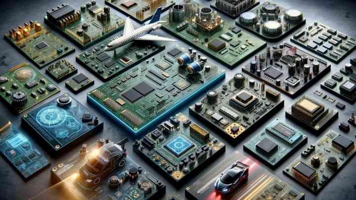
4. Custom PCBs in Different Industries
The adaptability of custom PCBs underscores their vital contribution across diverse industries. Each sector introduces distinct challenges, necessitating PCBs that are not merely operational but exceptionally specialized.
Aerospace: Soaring to New Heights with PCBs
Within the aerospace domain, PCBs transcend their conventional role, becoming the critical conduits of technology that must withstand the severe demands of both celestial and aerial environments. Creative Hi-Tech has underscored the imperative for PCBs that can tolerate the onslaught of extreme thermal variances and hostile conditions. The deployment of flexible, rigid, and rigid-flex PCBs in this realm is a deliberate choice, crafted to guarantee that satellites and aircraft perform impeccably, even in the most unforgiving circumstances.
Thermal Endurance: Aerospace-grade PCBs are constructed to resist the intense temperature fluctuations, from the icy void of space to the scorching friction of atmospheric re-entry.
Structural Tenacity: The chosen materials and architectural design are specifically fashioned to withstand the intense vibrations and shocks encountered during both launch and subsequent operations.y specialized.
Medical: Precision and Purity in PCB Design
The exigency for meticulously engineered PCBs within the medical sphere is unmatched. Pristine PCB assemblies are paramount, as they frequently integrate into apparatuses that are instrumental in critical care. The adoption of lead-free assemblies and stringent functional assessments is essential to align with the exalted standards of medical device production.
- Clean Assembly Environments: To prevent contamination, PCBs for medical devices are assembled in pristine conditions.
- Advanced Testing: Every PCB undergoes stringent testing to ensure reliability in critical medical applications.
Military: Durability in the Face of Adversity
For the military, failure is not an option. PCBs used in this sector must be robust enough to withstand harsh environments, from the blast of a jet engine to the depths of oceanic pressure. The military’s reliance on PCBs that can endure such conditions speaks volumes about the level of trust in these custom solutions.
- Ruggedness: Military PCBs are engineered to survive in the most challenging conditions without faltering.
- Comprehensive Testing: Rigorous testing protocols are in place to guarantee performance when it matters most.
Industrial Electronics: The Workhorses of PCBs
In the industrial electronics landscape, PCBs are the stalwart champions operating behind the scenes. They are embedded in a spectrum of apparatuses, from amplifiers to energy storage systems, each necessitating a PCB capable of sustained operation amidst diverse strains.
Dependability: Durability and steadfast performance are the distinguishing attributes of PCBs employed in this industry.
Resilience: PCBs utilized in military applications are crafted to endure the harshest of environments, ensuring unwavering functionality.
Thorough Validation: A stringent regimen of testing is enforced to affirm the PCB’s performance in pivotal moments.
Computing and Business Electronics: The Foundation of Functionality
The computer and business electronics sectors rely heavily on dependable PCBs as their cornerstone. These industries require PCBs that not only maintain consistent performance but also continually advance technological frontiers with each new version.
Unwavering Dependability: PCBs destined for these critical sectors are designed to withstand extended periods of intensive usage.
Pioneering Spirit: The relentless quest for superior, swifter, and more efficacious PCBs propels forward-thinking advancements in the realms of computing and commercial
5. The Design Process of Custom PCBs
The creation of a custom PCB is comparable to orchestrating a musical masterpiece; each element must resonate in perfect synchrony with the rest. The endeavor is complex, demanding profound insight into the electrical necessities as well as the specific exigencies of the intended application.
Conceptualization: The Blueprint of Innovation
The odyssey commences with a concept, a schematic vision of the desired outcome. This phase is dedicated to grasping the ‘why’ which precedes the ‘how’.
Needs Assessment: The process initiates with delineating the PCB’s required functionalities and limitations.
Practicality Evaluation: Subsequently, I examine tangible factors, including the accessibility of components and the financial ramifications.
Schematic Design: Crafting the Circuit’s DNA
Here, I translate the concept into a schematic diagram, which is essentially the DNA of the PCB. It’s a map that shows the connection between different components.
Component Curation: The selection of components is tailored not just to satisfy the electrical specifications but also to conform to the design’s spatial parameters.
Circuit Emulation: Prior to advancing to the physical configuration, I conduct simulations of the circuit to verify its operational integrity.
Layout Design: The Art of Placement
The layout stage is the juncture at which the PCB begins to manifest into a tangible form. It’s a painstakingly precise procedure where each millimeter is significant.
Component Footprint Arrangement: I meticulously position the outlines of the components, mindful of the current’s trajectory and the preservation of signal fidelity.
Trace Implementation: Subsequently, I delineate the pathways that will link the components, an endeavor that necessitates harmonizing electrical efficacy with the economical use of space.
Prototyping: Bringing the Design to Life
When the blueprint is established, the next crucial phase is to breathe life into a prototype. This pivotal step allows the design to be evaluated in a real-world context.
Prototype Fabrication: Employing swift prototyping methods, I craft a corporeal iteration of the PCB.
Trial and Refinement: The prototype is subjected to exhaustive trials. Any anomalies are rectified, and the design is polished for perfection.
Finalization: The Path to Production
With the prototype’s triumph, the design reaches its culmination. At this juncture, I ready the blueprint for large-scale manufacturing, ensuring every detail is meticulously conveyed to the fabricator.
Documentation: I compile comprehensive documentation that encompasses assembly schematics and guidelines.
Manufacturing Collaboration: I engage in a collaborative dialogue with the manufacturer to guarantee a thorough understanding of the PCB’s intricacies.
6. Material Considerations for Custom PCBs
Choosing the appropriate materials for a custom PCB is a decision that echoes through the device’s entire operational life. It transcends mere functionality; it’s about aligning the essence of the PCB with the core purpose of the application.
Substrate Selection: The Bedrock
The substrate serves as the PCB’s bedrock, with its material selection being pivotal. It’s not just a foundation; it’s the bedrock for electrical fidelity and structural solidity.
- FR4 PCB Material: My default choice is often FR4, the industry benchmark, lauded for its reliable electrical insulation and structural fortitude.
- High-Speed Materials: For scenarios where velocity is key, options like Megtron 6 are preferred for their reduced dielectric constants and dissipation factors, vital for preserving signal integrity at elevated frequencies.
Conductive Layers: The Vital Arteries
The conductive layers are akin to the PCB’s arteries, channeling signals and power throughout the board. Copper stands as the standard, yet its gauge and processing can differ substantially.
- Copper Weight: The copper’s heft influences its capacity to carry current and manage heat. The power demands of the application guide me in selecting the appropriate weight.
- PCB Surface Finish: The surface finish is also a consideration, be it HASL for cost efficiency or ENIG for enhanced conductivity and longevity. Learn about different surface finishes and their impact on your custom PCBs in our comparison of ENIG vs HASL
Solder Mask and Silkscreen: More Than Meets the Eye
While often perceived as merely cosmetic, the solder mask and silkscreen layers fulfill functional roles as well.
- Solder Mask: This coating safeguards the copper pathways from oxidization and averts solder bridging during assembly. I apply it meticulously for both protection and a polished appearance.
- Silkscreen: The silkscreen layer imparts human-readable inscriptions to the PCB. I apply it with restraint to facilitate assembly and diagnostics without overburdening the board.
Cost Considerations in Custom PCB Fabrication
Exploring the financial aspects of custom PCB manufacturing reveals a complex interplay of factors that shape the end cost. It’s a nuanced matrix of material selections and design decisions.
Material Choices: The Expenditure on Excellence
The choice of materials can markedly tip the cost scales. Superior substrates and specialized finishes command a higher price.
- Substrate Material: Choosing advanced materials like Rogers or Polyimide for high-speed or high-temperature applications can escalate costs beyond standard FR4.
- Copper Thickness: Opting for heftier copper layers to accommodate high-power needs also increases the financial outlay.
Complexity and Size: The Cost Correlation
The intricacy of the PCB design and the board’s dimensions are in direct correlation with the cost.
- Layer Count: Additional layers equate to increased complexity and expense. My objective is to strike a balance between functionality and fiscal prudence.
- Board Size: Expansive boards necessitate more material and can lead to manufacturing waste, thus affecting the cost.
Production Volume: The Economy of Scale
The production quantity can significantly influence cost efficiency. Smaller production runs incur higher per-unit costs due to setup expenses, whereas larger batches can amortize these costs more effectively.
- Prototyping vs. Mass Production: Prototyping carries a steeper unit cost but is an essential step for validation. Mass production benefits from the economy of scale.
Advanced Features: The Premium for Innovation
Incorporating sophisticated features like blind vias, buried vias, or microvias increases manufacturing complexity and, consequently, the cost.
- Innovative Techniques: Employing specialized methods such as via-in-pad or edge plating is costly but may be indispensable for high-density interconnect (HDI) designs.
7. Cost Factors in Custom PCB Manufacturing
The financial landscape of custom PCB manufacturing is a mosaic of influential factors that extend beyond the mere cost of materials or the expanse of the circuit board. It’s a nuanced interplay of strategic selections and concessions. While considering custom PCB solutions, understanding the PCB Cost Comparison can help you make informed budget decisions for your project
Material Selection: The Financial Implications of Excellence
The choice of materials can pivot the cost pendulum significantly. Premium substrates and specialized finishes command a higher price tag.
- Substrate Material: The election to use advanced materials such as Rogers or Polyimide, which cater to high-speed or high-temperature applications, can escalate costs in contrast to the conventional FR4.
- Copper Thickness: Opting for a denser copper layer to cater to high-power needs also contributes to the financial burden.
Design Intricacy and Board Dimensions: The Quest for Equilibrium
The complexity inherent in the PCB’s design and its overall size are in direct correlation with the cost.
- Layer Complexity: An increase in layer count denotes more complexity and, consequently, a rise in costs. Striking a balance between functional necessity and fiscal prudence is my constant goal.
- Board Proportions: Larger boards necessitate more material and can lead to increased waste during production, which can inflate costs.
Production Volume: The Economies of Scale
The volume of PCBs produced can significantly sway the cost-efficiency scale. Smaller batches incur higher per-unit costs due to fixed setup charges, whereas larger orders can amortize these expenses over more units, reducing the individual cost.
- Prototyping vs. Mass Production: Prototyping, while more costly on a per-unit basis, is an indispensable step for validation. Scaling up to mass production can capitalize on the economies of scale.
Advanced Features: The Premium of Innovation
The incorporation of advanced features such as blind vias, buried vias, or microvias introduces additional manufacturing complexity and, with it, additional costs.
- Innovative Techniques: Employing specialized methods like via-in-pad or edge plating, while financially demanding, may be essential for the intricate designs of high-density interconnect (HDI) PCBs.
8. Crafting Excellence: PCB Manufacturing at Finest Printed Circuit Board Ltd
Within the hallowed halls of Finest Printed Circuit Board Ltd, the creation of bespoke PCBs transcends mere production—it’s a symphony of precision harmonized with ingenuity, each board a masterpiece wrought with an unwavering commitment to detail.
Vanguard Fabrication Techniques
This bastion of PCB creation is a harbinger of the industry’s future, replete with avant-garde apparatus and methodologies.
- Sophisticated Apparatus: The adoption of the most recent automated and precision-focused machinery guarantees the birth of PCBs that adhere to the most exacting of blueprints.
- Stringent Quality Oversight: An exhaustive quality assurance protocol ensures that each board is synonymous with the excellence our clientele has come to anticipate.
Bespoke Production Odyssey
Every PCB narrative is singular, with a manufacturing odyssey sculpted to the narrative of the client’s requisites.
- Tailor-made Resolutions: From the genesis of material selection to the culmination of assembly, each phase is sculpted to dovetail with the project’s unique blueprint.
- Synergistic Client Alliance: An intimate alliance with our patrons ensures the transmutation of their conceptual vision into tangible excellence.
In the domain of tailor-made PCBs, Finest Printed Circuit Board Ltd is the paragon of quality and pioneering thought. For those in quest of a PCB solution that epitomizes precision and is bespoke to your distinctive necessities, your search culminates here.
Propel your inquiry forthwith, and together, let us navigate the odyssey of transfiguring your electronic conceptions into palpable innovation.