FR4 PCB

fr4-pcb

FR4 PCB
Board thickness: 1.6mm
Surface finish: ENIG
Layer: 4 layer

fr4-pcb-ENIG-blind-hole-4

FR4 PCB
Board thickness: 1.6mm
Surface finish:ENIG
Layer: 4 layer with bline hole

quick turn PCB manufacturing

FR4 PCB
Double Layer FR-4 PCBs
Surface Finish: ENIG
Thickness: 1.6mm

fr4 pcbs

FR4 PCB
Base Material: FR-4laminate
Layer: Four layer
Surface finished: HASL

fr4 pcb

FR4 PCB
Base Material: FR-4laminate
Layer: Double layer
Surface finished: HASL

fr4 pcb-ENIG- blind hole-4L

FR4 PCB
Board thickness: 1.6mm
Surface finish: ENIG
Layer: 4 layer

fr4 pcb

FR4 PCB
Base Material: FR-4laminate
Layer: Double layer
Surface finished: HASL

FR4 PCB

Introduction

When discussing Printed Circuit Boards (PCBs), one material often dominates the conversation: FR4. Renowned for its durability, electrical insulation, and thermal resistance, FR4 is the cornerstone of PCB fabrication — a silent sentinel in the relentless advance of electronic innovation. Yet, within this bastion of circuitry lies a variable of profound consequence, one that subtly dictates the performance, application, and longevity of the electronic components it supports: the thickness of the FR4 PCB.

The uninitiated might overlook the significance of PCB thickness, considering it a mere detail in the vast expanse of electronic design. However, those versed in the meticulous art of PCB engineering understand that thickness is a pivotal factor that harmonizes with the intricate dance of current, conductivity, and thermal management. It is a characteristic that demands careful consideration, a parameter that molds the very essence of electronic function across a multitude of sectors — from the delicacy of medical devices to the robust exigencies of aerospace engineering.

In this article, we will delve into a topic seldom tread upon with the detail it deserves — the judicious selection of FR4 PCB thickness. We will navigate through the layers of its impact, exploring how a millimeter’s variation can be the defining line between optimal performance and potential failure. This piece is not just a narrative on a technical specification; it is an odyssey across the vast landscapes where FR4 PCBs reside, each terrain with its own tale of thickness.

Section 1: The Basics of FR4 PCB

The domain of PCBs is as vast as it is intricate, but the foundations rest upon the shoulders of a material that is ubiquitously employed yet often not fully understood: FR4. Standing for “Flame Retardant level 4”, FR4 is not merely a static entity but a dynamic player in the world of circuitry. It is the canvas upon which electronic masterpieces are painted, and its properties are as pivotal as the components it interlinks.

Subsection 1.1: What is FR4?

FR4 is the nomenclature that has become almost synonymous with printed circuit board material. It is a composite of woven fiberglass cloth with an epoxy resin binder that is flame resistant (self-extinguishing). “What’s in a name?” one might ask. For FR4, it’s a blend of mechanical resilience and electrical insulation properties, a combination that is not chosen by chance but by a series of design deliberations that value longevity and performance.

Subsection 1.2: The Role of FR4 in PCB Design

In the alchemy of PCB design, FR4 serves as the quintessential base — a balancing act between cost-effectiveness and high-grade performance. Its thermal stability and dielectric strength are not just beneficial but critical for the varied environments that consumer electronics, automotive systems, and aerospace components encounter. Herein lies a seldom discussed facet: the nuanced selection of FR4 types. Beyond the standard grade, there exists an array of FR4 variations, each with modified attributes to better suit high-speed, high-frequency applications or to enhance thermal management. This selection process is a testament to the designer’s foresight and the application’s exigencies.

In this foundational section, we have just begun to scratch the surface of FR4’s role in PCBs. The true measure of this material’s worth is gauged not just by its ubiquitous presence but by its silent adaptability to the myriad demands of modern electronic devices.

Section 2: Deciphering PCB Thickness

The discourse on PCB thickness is often relegated to a footnote in the grand design manual of electronics. Yet, this parameter is a critical determinant of functionality, reliability, and even the very feasibility of a project. In the realm of FR4 PCBs, thickness is not a mere dimensional attribute but a pivotal decision point that influences the electrical and mechanical behavior of the final product.

2.1: Defining PCB Thickness

Thickness in the context of PCBs is more than a measurement; it’s a complex consideration that affects:

  • Signal integrity: The transmission of electrical signals without significant loss or distortion.
  • Thermal management: How well the board can dissipate heat generated by electronic components.
  • Mechanical stability: The board’s resistance to bending, which is crucial for both assembly and operation.

2.2: Standard Thicknesses of FR4 PCBs

While the standard thickness for PCBs is typically 1.57 mm, the range of FR4 substrate thickness is quite broad and can be as thin as 0.78 mm or as thick as 2.36 mm. This variability caters to a spectrum of applications, each with its own set of requirements and constraints. Here’s what influences the choice of thickness:

  • The nature of the electronic device: handheld gadgets versus stationary installations.
  • The physical environment: high vibration settings such as automotive or aerospace versus static environments like home appliances.
  • The need for flexibility versus rigidity in the end product.

2.3: Thickness Versus Flexibility

The dance between thickness and flexibility is a subtle art in PCB design. Consider the following:

  • Thicker boards provide a robust platform for heavyweight or high-power components but can sacrifice flexibility.
  • Thinner boards offer more flexibility, which is essential for certain applications but may have limitations in terms of component support and heat dissipation.

The decision matrix for FR4 PCB thickness is intricate, where one must weigh the merits of thickness against the demands of the project. The range of thicknesses from ten to three inches mentioned in the referenced guide underscores the breadth of customization available and the importance of precision in this choice.

In summary, when we talk about FR4 PCB thickness, we are engaging with a multifaceted element of design that goes beyond a mere number. It is a critical factor that must be tuned to the symphony of requirements each unique application plays. The selection of this dimension is a deliberate process, one that can dictate the success or failure of sophisticated electronic systems.

Section 3: Thickness Considerations for Specific Industries

The choice of FR4 PCB thickness cannot be made in a vacuum. It necessitates a deep understanding of the industry-specific challenges and requirements. This section peels back the layers of standard practice to reveal how thickness considerations can become pivotal in the success or failure of electronic products across various sectors.

3.1: Consumer Electronics

In the consumer electronics arena, the race for sleeker, more compact devices puts unique demands on PCB thickness. Thin FR4 PCBs are often favored for their ability to fit into slim profiles without compromising the integrity of the device. However, the selection process is tempered by:

  • The need for durability in handheld devices.
  • The heat generated by compact, high-performance components.

3.2: Automotive and Aerospace Applications

The automotive and aerospace industries require PCBs that can withstand extreme conditions:

  • Vibration resistance is paramount, often necessitating thicker FR4 PCBs for added structural integrity.
  • Thermal cycling, a common phenomenon in these industries, requires a thickness that ensures stability over a wide temperature range.

3.3: Medical and Industrial Equipment

In medical and industrial applications, reliability is non-negotiable. PCB thickness must be chosen to ensure:

  • Reliability over prolonged usage, with thicker PCBs often providing the needed robustness.
  • Compliance with stringent safety standards, where a thicker FR4 substrate can offer better insulation properties.

3.4: Telecommunications and Computing

The telecommunications and computing industries are battlegrounds for signal integrity and heat management. PCB thickness plays a crucial role:

  • Thicker PCBs can support larger, heat-dissipating components necessary for high-speed computing.
  • Balancing thickness with the need for multi-layered boards that can handle complex routing and high signal integrity.

3.5: Renewable Energy and Power Systems

In the renewable energy and power sectors, the robustness of FR4 PCBs is tested against the elements:

  • Thicker PCBs are often utilized to endure the physical stresses of outdoor environments.
  • The ability to conduct heat away from critical components without warping is a key consideration in selecting the appropriate thickness.

Section 4: Advanced Considerations in FR4 PCB Thickness

The dialogue on FR4 PCB thickness often revolves around its impact on the basic functionality of the board. However, when we venture into the realm of advanced applications, thickness takes on a far more nuanced role, influencing not just the performance but also the innovation and future-readiness of the PCB.

4.1: Multi-layer PCBs and Thickness

For multi-layer PCBs, each additional layer is a new frontier in complexity. Here, thickness is a balancing act between electrical performance and physical constraints. Advanced considerations include:

  • Interlayer connectivity: Optimal thickness ensures reliable via connections between layers.
  • Signal integrity: Careful planning of the PCB thickness can mitigate issues like crosstalk and electromagnetic interference (EMI).

Consider the case of a high-frequency communication device. The device’s performance is critically dependent on the precise calibration of the PCB’s thickness to ensure signal clarity and strength.

Subsection 4.2: Thermal Management and Thickness

Effective thermal management is a cornerstone of advanced electronics, especially in high-power applications. The FR4 PCB thickness influences:

  • Heat dissipation: Thicker boards can provide better heat distribution, but may also require additional cooling strategies.
  • Component spacing: Thicker boards may allow for greater component spacing, which aids in heat management.

A quote from a seasoned PCB designer, “In our high-power designs, selecting the right PCB thickness isn’t just a technical decision; it’s an art that balances thermal efficiency with mechanical stability.”

Subsection 4.3: Future Trends in FR4 PCB Thickness

Looking forward, the trends in PCB thickness are shaping the frontier of electronics:

  • Thinner is not always better: The drive towards miniaturization is being recalibrated with the understanding that thermal and mechanical performance must not be sacrificed.
  • Custom thickness profiles: We’re seeing a rise in custom thickness profiles within a single PCB to cater to specific component needs.

Innovation Spotlight: A recent breakthrough in multi-thickness PCBs allowed for the integration of high-frequency and high-power circuits within the same board, without compromising on performance or size.

In sum, advanced considerations in FR4 PCB thickness underscore the material’s role as a silent yet powerful influencer in the evolution of PCB technology. As we push the boundaries of what’s possible, the thickness of FR4 PCBs will continue to be a bolded word in the lexicon of electronics innovation.

Conclusion

We have journeyed through the microscopic layers of FR4 PCBs, uncovering the pivotal role of thickness in the vast landscape of electronic applications. From the tight confines of consumer gadgets to the expansive realms of aerospace and automotive technology, the choice of PCB thickness is not a mere technicality but a strategic decision that molds the future of electronic innovation.

As we have seen, FR4 PCB thickness influences everything from signal integrity and thermal management to mechanical robustness and industry compliance. This choice is a dialogue between the present needs and future demands, a balance of performance, cost, and durability that requires foresight and expertise.

For those at the helm of creating the next wave of electronic marvels, we extend an invitation to delve deeper into the world of FR4 PCBs with Finest Printed Circuit Board Ltd. Our two decades of experience stand as a testament to our commitment to precision, quality, and innovation in PCB manufacturing.

Whether you are designing for the delicate intricacies of medical devices or the robust needs of industrial equipment, let us assist you in navigating the complexities of PCB thickness. Together, we can craft PCBs that not only meet but exceed the demands of your industry.

Embark on a collaborative journey with us, where each micron of thickness is calculated with precision to ensure your product’s excellence. Reach out to Finest Printed Circuit Board Ltd for your next project and experience a partnership that brings your vision to life with unmatched technical acumen.

Inquire about our PCB solutions today and elevate your products to new heights of innovation and reliability.

Advanced Considerations in FR4 PCB Thickness
AspectConsiderationImpact
Multi-layer PCBsThickness determines interlayer connectivity and signal integrityEssential for high-frequency communication devices
Thermal ManagementThickness affects heat dissipation and component spacingCrucial for high-power applications
Future TrendsEvolution towards custom thickness profilesEnables integration of diverse circuit functions
Please enable JavaScript in your browser to complete this form.
Name

Exploring the World of FR4 PCBs

 FR4 PCB General Capabilitiesfr4 pcb
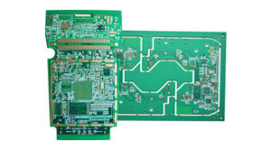
Definition and explanation of FR4 PCBs.

FR4 material is a PCB substrate that comes in the form of epoxy-reinforced glass fiber laminates. Due to its rugged nature and flame retardant properties, it is a common laminated substrate in printed circuit boards. Therefore, it is essential to provide the required insulation for the board. FR4 PCBs, an essential cornerstone of the PCB manufacturing process, refer to Printed Circuit Boards that are crafted using a composite material known as FR4. This material’s acronym originates from “Flame Retardant 4,” highlighting its remarkable resistance to combustion and its role in enhancing safety in the realm of PCB manufacturing process.

In the intricate landscape of PCB manufacturing, FR4 material serve as the very canvas upon which the intricate tapestry of electronic components is meticulously woven. They provide the structural foundation necessary to support, interconnect, and power the various components that collectively breathe life into an extensive array of electronic devices. These circuit boards play a pivotal role in connecting and powering electronic components, ensuring the seamless functioning of countless devices that define our digital age.

The composition of FR4 material is a well-engineered blend of materials that combine to offer the desired electrical, thermal, and mechanical characteristics. At its core is an epoxy resin matrix infused with woven fiberglass. This combination grants the PCB its rigidity and strength, allowing it to withstand the demands of various applications. Copper foil layers are bonded to the substrate, creating conductive pathways that enable the flow of electrical signals.

At its core lies an epoxy resin matrix seamlessly interwoven with layers of fiberglass. This marriage of materials results in a substrate that boasts impressive mechanical durability, perfectly suited for the exacting demands of the PCB manufacturing
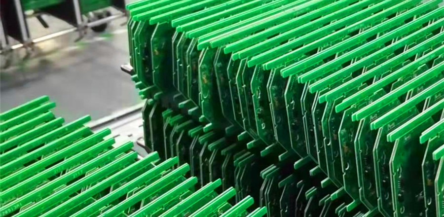
FR4 PCBs

Properties of FR4 PCBs

FR4 material PCBs, integral to the world of PCB manufacturing, boast a spectrum of properties that make them a sought-after choice in electronic design. As an essential constituent of the PCB manufacturing materials landscape, FR4 offers a unique blend of attributes that contribute to its widespread use, cost-effectiveness, and versatility.

Electrical Properties:

FR-4 exhibit consistent electrical characteristics, making them well-suited for a range of applications. Their dielectric constant and loss tangent facilitate effective signal propagation, a critical factor in high-frequency circuits. This makes FR-4 PCBs valuable in industries that demand reliable data transmission and communication.

Thermal Properties:

While not the most thermally conductive material, FR-4 PCBs effectively manage heat generated by electronic components during the PCB manufacturing process. Their ability to dissipate heat helps maintain the stability of circuits and prevents performance degradation due to excessive temperatures.

FR-4 exceptional tensile and flexural strength lend them durability, ensuring they can withstand the rigors of handling, assembly, and operation. This resilience extends the lifespan of devices and contributes to their reliability, a paramount consideration in the PCB manufacturing process.

Chemical Resistance:

FR-4 PCBs exhibit resistance to chemicals, solvents, and moisture, a vital characteristic for maintaining performance and reliability over time. This property safeguards devices against environmental factors and contributes to their longevity.

Balancing PCB Manufacturing Costs:

FR-4 PCBs are favored not only for their technical attributes but also for their cost-effectiveness. In the realm of PCB manufacturing costs, the availability and wide use of FR4 materials contribute to their affordability. Their balanced combination of performance and price point makes them an attractive choice, especially for applications where optimizing PCB manufacturing price is crucial.

The general technical indicators of FR-4 sheet material are: bending strength, peeling strength, thermal shock performance, flame retardant performance, volume resistance coefficient, surface resistance, dielectric constant, dielectric loss Angle tangent, glass transition temperature Tg, dimensional stability, maximum service temperature, warpage degree, etc.

Dielectric Constant and Loss Tangent

FR4’s dielectric properties influence signal propagation and integrity, making it suitable for high-frequency applications.

Glass Transition Temperature (Tg)

FR4 maintains its mechanical strength and stability even at elevated temperatures, ensuring reliability in demanding conditions. The most obvious difference between FR-4 materials is the Tg value, according to the Tg temperature, FR-4 plates are generally divided into low Tg, medium Tg and high Tg plates. In the industry, FR-4 Tg of about 135℃ is usually classified as low Tg sheet; The FR-4 of Tg at about 150℃ is medium Tg plate; FR-4 Tg at about 170℃ is classified as high Tg plate.

If the PCB is processed with more times of pressing, or more PCB layers (more than 14 layers), or the welding temperature is high (≥230℃), or the working temperature is high (more than 100C), or the welding thermal stress is large (such as wave welding), high Tg plate should be selected.

Tensile and Flexural Strength

FR4’s robust mechanical properties offer resistance against bending, impact, and other stresses.

Applications of FR4 PCBs

As a cornerstone of modern electronics, find themselves at the heart of a diverse range of applications. Their versatile nature, compatibility with Multilayer PCB designs, and integral role in the PCB manufacturing process have solidified their position across various industries, from consumer electronics to cutting-edge technology. They had applicated in many different electronic area.

Consumer Electronics PCB: FR4 are the unsung heroes within our gadgets. In smartphones, tablets, and laptops, they enable seamless connectivity, data processing, and power distribution. As Multilayer PCB designs become increasingly prevalent, FR4 material accommodate the intricate circuitry required by these devices. The integration of various components within compact spaces is a testament to their efficiency.

Industrial Control PCB: In the realm of industrial automation, it play a pivotal role in control systems, robotics, and factory automation. These applications demand precision and reliability, both of them deliver. Their mechanical stability, resistance to environmental factors, and adaptability to the complexities of PCB manufacturing automation make them a cornerstone of industrial progress.

Automotive PCB: Contribute to the advancement of automotive technology. They power engine control units (ECUs), infotainment systems, safety features, and navigation systems. The intricate Multi-Layer PCBs in these applications necessitate a material that can facilitate the complex interconnections required for modern vehicles.

Telecommunications PCB: Routers, switches, and communication devices rely on High performanc PCBs to maintain connectivity in the digital age. These intricate networks demand high-performance Multilayer PCBs to ensure data transmission efficiency and reliability. FR4’s properties enable the construction of robust and dependable communication systems.

PCB Assembly Service and Rapid Prototyping: FR4 play a crucial role in the PCB assembly service landscape. Their compatibility with automated assembly processes streamlines production, ensuring efficient and cost-effective manufacturing. Moreover, in PCB rapid prototyping, FR4 enable designers to iterate and refine their designs swiftly, allowing for faster time-to-market for new products.

As technology evolves, the applications of Advanced PCB manufacturing continue to expand. Their role in Multilayer PCB designs, coupled with their contribution to PCB manufacturing automation and rapid prototyping, positions them as an indispensable asset in the realm of modern electronics.
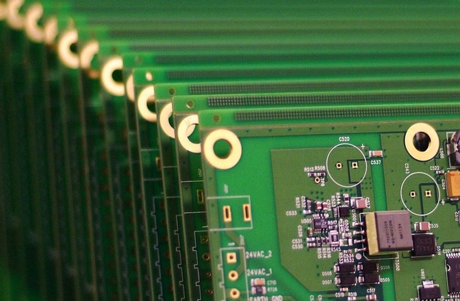
FR4 PCB

FINEST Pinted Circuit Board Ltd is a subsidiary of FINEST Group. It was established on April 2019, specializing in EMS Processing, SMT quick-turn prototype and small batch production. Finest PCBA team with the ability to selecting materials, making samples and small batch production, and donging testing services. We always improve research and development efficiency, aiming at providing fast service to satisfies customers’ different demands for PCB assembly. Free to send us your file for quote, we ill resonse you within 24 hours.https://finestpcb.com/contact/

[contact-form-7 id=”6d2906f” title=”Contact form”]

  • Single Sided PCB
  • Double Sided PCB
  • Multi-Layer PCB
  • Buried Via PCB
  • Blind Via PCB
  • Impedance Controlled PCB
  • Micro Via PCB
  • Laser Drilling PCB
  • RoHS Compliance PCB
  • Epoxy filled vias PCB

FR4 PCB Specific Capabilities

Attribute: see (*) below as applies

S/Sided

D/Sided

Multilayer

Advanced

Minimum Line/Spacing, Internal Layer

N/A

N/A

.004”/.004”

.003”/.003”

Minimum Line/Spacing, External Layer

.007”/.008”

.007”/.008”

.005”/.005”

.003”/.003”

Aspect Ratio (Thickness to Drill)

6:1

6:1

8:1

10:1

Minimum Drilled Hole Size

.010”

.008”

.008”

.008”

Land Size Internal (Diameter Over Drill)

N/A

N/A

.015”

.012”

Land size External (Diameter Over Drill)

.012”

.012”

.012”

.010”

Plane Clearance (Diameter Over Drill)

.030”

.030”

.030”

.024”

Plated Hole Tolerance

+/- .003”

+/- .003”

+/- .003”

+/- .002”

Minimum Dielectric Thickness

N/A

N/A

.0025”

.002”

Minimum Core Thickness

N/A

N/A

.004”

.003”

Minimum PCB Thickness **

.017”

.018”

.020”

.020”

Maximum PCB Thickness

.125”

.125”

.250”

.250”

Thickness Tolerance (%)

+/- 10

+/- 10

+/- 10

+/- 5

Maximum Board Dimensions *

16” x 52”*

19” x 22”*

17” x 23”*

17” x 23”*

Fabrication Tolerances (overall dimension)

+/- .010”

+/- .010”

+/- .010”

+/- .005”

Bow and Twist (Through Hole) %

1.5

1.5

1.5

1

Bow and Twist (SMT) %

.75

.75

.75

.75

Minimum Conductor to Edge

.015”

.015”

.015”

.010”

Layer to Layer Registration Tolerance

N/A

.004”

.004”

.003”

Component Pitch

.025”

.025”

.025”

.015”

Soldermask Clearance

.005”

.005”

.005”

.004”

Soldermask Dams

.005”

.005”

.005”

.004”

Impedance Tolerance (>50 Ohms) %

+/- 10

+/- 10

+/- 10

+/- 8

Maximum Layers

1

1

12

16

Minimum Copper Weight Inners (oz.)

N/A

N/A


1/4

Maximum Copper Weight Int. Ground (oz.)

N/A

N/A

3

8

Maximum Copper Weight Int. Signal (oz.)

N/A

N/A

2

6

Maximum Copper Weight Ext. Ground (oz.)

4

4

2

10

Maximum Copper Weight Ext. Signal (oz.)

4

4

3

10