Comprehensive Guide to PCB Prototype Fabrication Service
Introduction to PCB Prototype Fabrication Service
When it comes to developing electronic devices, the quality and precision of the PCB (Printed Circuit Board) can make or break your project. PCB prototype fabrication services offer a critical step in transforming your design into a tangible, functional product. Whether you’re an engineer, a hobbyist, or a company looking to bring a new device to market, understanding the intricacies of PCB prototype fabrication is essential.
Understanding the PCB Fabrication Process
What is PCB Fabrication?
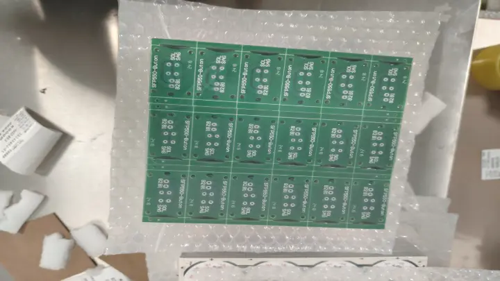
PCB fabrication involves creating a physical circuit board from a digital design. This process includes several steps to ensure that the final product meets the required specifications and performs reliably.
PCB Fabrication Process Steps
- Design and Layout: This initial stage involves using CAD software to design the PCB layout. Engineers create a schematic of the electronic circuit, specifying where each component will be placed. The design must account for electrical properties and physical constraints.
- Photomasking: The design is transferred onto a photographic film to create a mask. This mask is then used to expose the board to UV light, hardening the photoresist on areas where copper should remain. The unexposed areas are then washed away, preparing the board for etching.
- Etching: Unwanted copper is removed from the board to reveal the circuit pattern. The board is submerged in an acid solution that dissolves the exposed copper, leaving behind only the desired circuitry. This step is crucial for defining the electrical paths on the PCB.
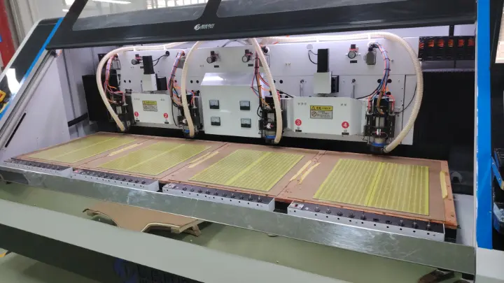
- Drilling: Precise holes are drilled for component placement. These holes allow electrical connections between different layers of the PCB and provide mounting points for components. The drilling process requires high precision to ensure alignment with the design.
- Plating and Solder Masking: Conductive plating is added, and a solder mask is applied to protect the board. Plating the holes with copper ensures reliable electrical connections, while the solder mask prevents short circuits and corrosion by covering the non-conductive areas.
- Testing: Rigorous tests are performed to ensure the board functions as intended. Electrical tests check for continuity and isolation between circuits, while visual inspections verify the physical integrity of the board. This step is essential for quality assurance.

Cost Considerations in PCB Fabrication
PCB Fabrication Price
The cost of PCB fabrication can vary significantly based on factors such as complexity, materials, and quantity.
- Simple PCBs: Typically lower cost due to straightforward designs. These boards might have a single layer or a basic double-layer design, making them less expensive to produce. They are ideal for simple electronics projects and prototypes.
- Complex PCBs: Higher cost due to intricate designs and additional layers. Multi-layer PCBs require more sophisticated manufacturing processes and materials, which increase the cost. They are used in advanced electronics like smartphones and computers.
- Bulk Orders: Reduced unit cost due to economies of scale. Ordering a large quantity of PCBs at once can significantly lower the cost per unit. This is beneficial for mass production, where the initial setup costs are spread over many units.
PCB Fabrication Cost Breakdown
- Material Costs: High-quality materials, like FR4, increase costs. FR4 is a common PCB material known for its good thermal and electrical properties. Using specialized materials, such as high-frequency substrates, can further drive up costs.
- Labor Costs: Skilled labor and advanced machinery contribute to the expense. Precision in fabrication requires experienced technicians and sophisticated equipment, which add to the overall cost of production.
- Testing and Quality Control: Ensures reliability but adds to the overall cost. Extensive testing procedures, such as electrical and functional tests, are necessary to guarantee the performance and durability of the PCBs. These tests require specialized equipment and expertise.

PCB Prototype Fabrication
How Much Does It Cost to Prototype a PCB?
Prototyping costs can range widely based on the design’s complexity and the number of layers involved.
- Single-Layer PCBs: More affordable due to simpler construction. These prototypes are suitable for basic circuits and initial concept testing, providing a cost-effective way to validate designs before investing in more complex boards.
- Multi-Layer PCBs: More expensive due to additional processes and materials. These prototypes are used for complex designs that require multiple layers to accommodate dense circuitry and high-performance requirements. The increased cost reflects the advanced manufacturing techniques needed.
- Turnaround Time: Faster service often incurs higher costs. Rapid prototyping services can deliver PCBs in a matter of days, but this expedited process typically comes with a premium price. It is ideal for time-sensitive projects where quick feedback is essential.
Benefits of PCB Prototyping
- Design Validation: Ensures the design functions correctly before mass production. Prototyping allows engineers to test and refine their designs, catching any errors or inefficiencies early in the development process.
- Error Detection: Identifies and rectifies design flaws early. By building and testing a prototype, issues such as incorrect component placement, signal interference, or thermal management problems can be identified and resolved before committing to full-scale production.
- Performance Testing: Assesses how the PCB performs under real-world conditions. Prototyping provides an opportunity to test the board’s functionality and durability in the environment it will be used, ensuring it meets the necessary performance standards.
PCB Assembly and Its Costs
How Much Does It Cost to Get a PCB Assembled?
PCB assembly costs depend on factors such as component types, board complexity, and assembly methods.
- Surface-Mount Technology (SMT): Generally cheaper due to automation. SMT allows for rapid and efficient placement of components on the PCB, reducing labor costs and increasing production speed. It is ideal for high-volume manufacturing.
- Through-Hole Technology: Often more expensive due to manual labor. This method involves placing components through holes in the PCB and soldering them by hand or machine, which is more labor-intensive. It is typically used for components that require strong mechanical bonds.
- Mixed Technology: Involves both SMT and through-hole, affecting costs. Some PCBs use a combination of both technologies to optimize performance and reliability. This hybrid approach can be more costly due to the need for multiple assembly processes.

Why is PCB Assembly So Expensive?
- Component Costs: High-quality or rare components can increase costs. Components with specific tolerances, high performance, or unique properties tend to be more expensive. Ensuring the availability and compatibility of these components adds to the cost.
- Labor and Equipment: Advanced machinery and skilled labor add to expenses. High-precision assembly machines and experienced technicians are necessary for producing reliable and high-quality PCBs. This infrastructure investment is reflected in the assembly cost.
- Quality Assurance: Extensive testing to ensure reliability contributes to the overall cost. Quality assurance involves multiple stages of testing, including automated optical inspection (AOI), X-ray inspection, and functional testing. These processes ensure the PCB meets all specifications and performance criteria.
PCB Cloning and Life Expectancy
How Much Does PCB Cloning Service Cost?
PCB cloning involves replicating an existing PCB design, and costs can vary based on complexity and the level of reverse engineering required.
- Simple Designs: Less expensive due to straightforward replication. Cloning a basic PCB with few components and layers is typically more affordable. It involves copying the layout and electrical pathways, which is relatively simple.
- Complex Designs: Higher costs due to intricate circuits and components. Cloning multi-layer PCBs with complex circuitry requires advanced techniques and more time, increasing the cost. These designs often involve high-density components and specialized materials.
- Reverse Engineering: Adds to the cost if detailed analysis is needed. When the original design files are unavailable, reverse engineering is necessary to recreate the PCB layout. This process involves analyzing the existing board, which can be time-consuming and costly.
What is the Life Expectancy of a PCB?
The lifespan of a PCB depends on factors such as usage, environment, and quality of materials.
- High-Quality Materials: Longer lifespan due to durability. Using robust materials like high-temperature laminates and gold-plated contacts can significantly extend the life of a PCB. These materials resist wear and environmental stress better than lower-quality options.
- Proper Usage: Avoiding excessive heat and stress can extend life. Ensuring the PCB operates within its specified temperature and electrical limits prevents damage and prolongs its functional life. Proper handling during installation and maintenance is also crucial.
- Regular Maintenance: Ensures longevity and optimal performance. Regular inspections and cleaning can prevent issues such as corrosion and thermal damage. Identifying and addressing potential problems early helps maintain the board’s functionality over time.
Timeline for PCB Fabrication
How Long Does It Take to Fabricate a PCB?
The time required for PCB fabrication can range from a few days to several weeks.
- Simple Designs: Faster turnaround due to less complexity. Basic single-layer or double-layer PCBs can often be fabricated quickly, typically within a few days. These designs require fewer steps and less intricate processing.
- Complex Designs: Longer fabrication time due to intricate processes. Multi-layer PCBs with advanced features, such as embedded components or high-density interconnects, take longer to fabricate. The additional layers and processes require more time for precision and accuracy.
- Express Services: Available for urgent projects, typically at a higher cost. Many fabrication services offer expedited options for time-sensitive projects. While these services ensure faster delivery, they usually come at a premium price to accommodate the rush.

FAQs
How much does it cost to prototype a PCB? The cost varies widely, ranging from $50 for simple single-layer prototypes to several thousand dollars for complex multi-layer designs.
How much does it cost to get a PCB assembled? Assembly costs can range from $30 for simple boards using SMT to hundreds of dollars for complex designs requiring manual assembly and testing.
How much does PCB cloning service cost? PCB cloning costs typically start around $100 for simple designs and can exceed $1000 for complex, multi-layer boards with numerous components.
What is the life expectancy of a PCB? PCBs can last anywhere from 5 to 20 years, depending on usage conditions, quality of materials, and maintenance practices.
How long does it take to fabricate a PCB? Fabrication times can range from 3 days for simple designs to several weeks for complex, multi-layer boards.
Why is PCB assembly so expensive? Costs are driven by the need for high-quality components, advanced assembly equipment, skilled labor, and rigorous testing to ensure reliability.


