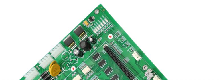

How to Choose USB PCB Board?

The charging USB PCB board is the center for the USB connecting interface gadgets due to its popular usage. It aids in transmitting data quickly in an efficient way.
Different brands of USB 2.0 are in the market space, but the use of its application becomes difficult. This is due to a series of challenges posed by the USB design after assembling the USB keyboard circuit.
Designing a PCB that satisfies the 2.0 USB demands is very vital for the designed brand’s integrity.
The USB power bank PCB compactness explains the relaying of the electrical signals by various lines (D+, D-). For the USB gadget to perform maximally, the distinctive lines designed must agree to guiding rules.
In fixing the elements on the USB switch PCB, the distinctive lines must be as short as they could be. Plan the distinctive lines at first so that they will not exceed two vias. The vias enhance the parasitic inductor of the lines that in turn affect the signal strength.
The USB 2.0 device uses three types of speed. The peripheral gadgets that include Keyboards, and mice are low-speed gadgets. They run at a speed of 1.5mbit/s to transfer data whereas high-speed gadgets transfer data at a speed of 12 mbit/s.
These high-speed USBs are always used by gadgets that use hard drives. To get a full-speed operation from high-speed gadgets, identification with the host is vital.