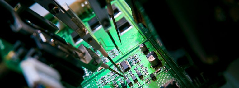

What are the Requirements of the PCB Manufacturing Process for Pads?

The pad is the basic unit of PCB surface mount assembly. So, do you know what the PCB manufacturing process requires for pads?
1. Test points should be added to the pads where the two ends of the chip components are not connected to the plug-in components. The diameter of the test points is equal to or greater than 1.8mm to facilitate the online tester test.
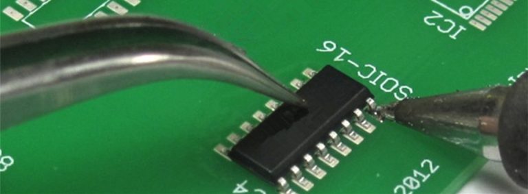
2. For IC pin pads with dense pin spacing, if they are not connected to the hand plug-in pads, test pads need to be added. The diameter of the test point is equal to or greater than 1.8mm to facilitate online tester testing.
3. If the distance between the pads is less than 0.4mm, white oil must be applied to reduce continuous soldering when the wave crest is exceeded.
4. The two ends and ends of the SMD component should be designed with lead-tin, and the lead-tin width is recommended to use 0.5mm wire, and the length is generally 2 or 3mm.
5. If there are hand-soldering components on the single-side electronic circuit board, remove the tin bath, the direction is opposite to the soldering direction, and the width of the hole is 1.0mm to 0.3mm.
6. The spacing and size of the conductive rubber keys should be consistent with the actual conductive rubber keys, and the connected ones should be designed as gold fingers, and the corresponding gold plating thickness should be specified.
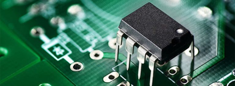
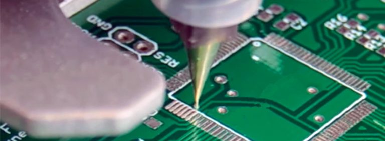
7. The size and spacing of the pad should be exactly the same as the size of the patch component.