
Can Multilayer PCBs Change the World? Exploring Their Impact on 5 Key Points
Imagine a world where electronic devices are lighter, thinner, and more powerful than ever before. A world where complex circuits can be squeezed into tiny spaces, enabling groundbreaking advancements in healthcare, communication, and beyond. This is the reality unlocked by the wonders of multilayer PCBs.
These intricate marvels of engineering, often hidden beneath the sleek surfaces of our gadgets, are revolutionizing the way we interact with technology. But have you ever stopped to wonder: what exactly are multilayer PCBs, and how do they work their magic?
Delve deeper with us on this exciting journey as we unveil the secrets of these layered wonders. We’ll peel back the layers (pun intended!), exploring their intricate design, diverse applications, and the fascinating manufacturing processes that bring them to life.
Demystifying Multilayer PCBs: Unveiling the Layered Wonders
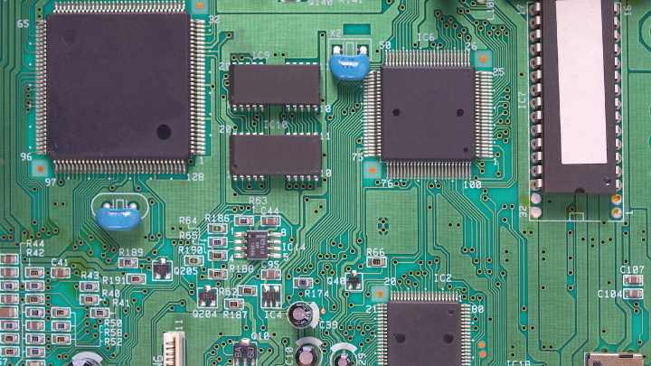
Imagine a tiny, intricate sandwich stacked with layers of conductive copper, insulating materials, and connecting vias. This isn’t your average lunchtime fare, but the fascinating world of multilayer PCBs. Forget chunky single-layer boards, these multi-layered marvels are revolutionizing electronics by packing more functionality into smaller spaces.
What are Multilayer PCBs?
Think of a complex city with multiple levels of roads, buildings, and utilities. Multilayer PCBs operate on a similar principle. Instead of just two sides like traditional PCBs, they boast three or more conductive copper layers, each separated by thin insulating layers. These layers are interconnected by tiny holes called vias, allowing signals to flow between them, creating a compact and powerful electronic backbone.
But how many layers exactly? While simple designs might have 4-6 layers, complexity reigns supreme. High-performance smartphones, for instance, can contain a staggering 12-16 layers, while some cutting-edge aerospace applications push the boundaries with over 40 layers! Each layer serves a specific purpose, carrying signals, power, or ground, working together to orchestrate the electronic symphony within your devices.
Understanding the Building Blocks: Layers, Materials, and Connections
Let’s delve deeper into the building blocks of these layered wonders:
- Layers: The heart of the matter, these copper layers are coated with a thin layer of gold or another protective material to ensure conductivity and prevent corrosion. Each layer carries specific signals or power, like dedicated lanes on a highway.
- Insulating Materials: Separating the conductive layers are thin sheets of insulating materials like FR4 or polyimide. These act as electrical barriers, preventing unwanted current flow and ensuring signal integrity. Imagine them as traffic dividers keeping everything organized and flowing smoothly.
- Vias: Tiny holes drilled through the board, plated with conductive metal, become the crucial connection points between layers. Think of them as tunnels or bridges allowing signals to travel vertically through the PCB’s “cityscape.” Depending on the design, vias can be “plated through-hole” (connecting all layers) or “blind/buried” (connecting specific layers), offering flexibility and design optimization.
The choice of materials plays a crucial role in performance and cost. Standard FR4 offers affordability and good electrical properties, while high-performance applications might utilize polyimide for its superior thermal resistance. The number of layers, chosen materials, and via configurations all contribute to the unique characteristics and capabilities of each multilayer PCB.
Fun Fact: Did you know the thickness of a single layer can be as thin as 0.001 inches (0.025 mm)? That’s about the width of a human hair! This incredible miniaturization allows for packing more functionality into smaller devices, a key driver of modern electronics.

Comparing Multilayer PCBs to Single-Layer Designs: Unveiling the Advantages
For decades, single-layer PCBs served as the workhorses of the electronics industry. But as technology advanced, demanding more complex circuits and smaller form factors, the limitations of single-layer designs became apparent. Enter the stage: multilayer PCBs, revolutionizing the game with their layered architecture and numerous advantages.
Unveiling the Advantages: Why Multilayer PCBs Reign Supreme
While single-layer PCBs offer simplicity and affordability for basic applications, multilayer PCBs bring a plethora of benefits to the table:
1. Compact Design: Imagine cramming a city’s worth of infrastructure into a single building. That’s the magic of multilayer PCBs! By stacking layers, they achieve significantly smaller footprints compared to single-layer designs, making them ideal for space-constrained devices like smartphones and wearables.
2. Enhanced Functionality: Think of a single-lane highway versus a multi-lane freeway. Multilayer PCBs offer increased routing flexibility thanks to their multiple layers, allowing for more complex circuits and components to be integrated within the same board area. This translates to more features and functionalities packed into your devices.
3. Improved Performance: The layered architecture of multilayer PCBs enables optimized signal routing and reduced signal interference, leading to faster data transfer speeds and enhanced signal integrity. This translates to smoother performance, especially in high-frequency applications.
4. Reduced Electromagnetic Interference (EMI): With multiple ground planes and controlled impedance, multilayer PCBs provide superior EMI shielding, protecting sensitive electronic components from external noise and ensuring reliable operation in complex environments.
5. Increased Design Flexibility: The layered structure unlocks a world of design possibilities. Multilayer PCBs allow for independent routing of power, ground, and signal layers, simplifying layout and optimizing performance. This flexibility empowers engineers to create more sophisticated and innovative electronic devices.
Real-World Example: Consider a modern inverter PCB. A single-layer design might struggle to accommodate the complex circuitry and power requirements. However, a multilayer PCB with dedicated power and ground planes, optimized routing, and EMI shielding can deliver efficient power conversion, minimize noise interference, and ensure reliable performance in a compact form factor.
Statistics: The demand for multilayer PCBs is on the rise, driven by miniaturization trends and increasing device complexity. The global market for multilayer PCBs is expected to reach a staggering $31.6 billion by 2027, highlighting their growing significance in the electronics industry.
Exploring Different Types: Rigid, Flexible, and Rigid-Flex Options
Multilayer PCBs aren’t a one-size-fits-all solution. Each type shines in specific applications, offering unique advantages and considerations:
1. Rigid Multilayer PCBs:
- Built for Stability and Durability: Imagine the robust frame of a building. Rigid multilayer PCBs, typically constructed with FR4 or similar materials, offer a solid foundation for demanding applications like industrial controllers, medical equipment, and computers. Their strength ensures reliable performance under stress and heat, making them ideal for environments where stability is paramount.
- Thermal Management Champions: Rigidity comes with a perk – efficient heat dissipation. Rigid PCBs excel at conducting heat away from sensitive components, thanks to their larger surface area and ability to integrate heat sinks. This makes them suitable for applications generating significant heat, like power supplies and high-performance electronics.
- Cost-Effective Choice: Due to their simpler manufacturing process compared to flexible options, rigid PCBs offer a budget-friendly solution. For applications where flexibility isn’t a requirement, their affordability makes them a popular choice for various electronic devices.
2. Flexible Multilayer PCBs:
- Bending the Rules of Electronics: Unlike their rigid counterparts, flexible multilayer PCBs boast a bendable base material like polyimide, allowing them to adapt and conform to diverse shapes and spaces. This makes them perfect for applications like wearables, medical implants, and even robotics, where movement and space constraints are key considerations.
- Lightweight and Compact Design: Imagine a feather-light phone that flexes in your pocket without breaking. Flexible PCBs, due to their thin and lightweight nature, are ideal for weight-sensitive applications like drones and aerospace components. This weight reduction translates to improved performance and efficiency, particularly in battery-powered devices.
- Higher Price Point: The complex manufacturing process and specialized materials involved in creating flexible PCBs contribute to a higher cost compared to rigid options. However, their unique capabilities often outweigh the price consideration for applications where flexibility is essential.
3. Rigid-Flex Multilayer PCBs:
- Ultimate Versatility: Imagine a phone antenna that bends with your movements while maintaining a rigid base for connectivity. Rigid-flex PCBs combine the best of both worlds, offering rigid sections for stability and flexible areas for movement. This versatility makes them perfect for demanding applications like robotics, aerospace, and even advanced wearables where both rigidity and flexibility are crucial.
- Engineered for Complexity: Integrating rigid and flexible sections within a single board requires advanced design and manufacturing techniques. This complexity translates to a higher cost compared to both rigid and flexible options alone. However, for applications where their unique properties are irreplaceable, the cost is justified by the unmatched performance and functionality they offer.
- Tailored Solutions: Rigid-flex PCBs can be customized with varying degrees of flexibility and rigidity within the same board, catering to the specific needs of each application. This level of customization allows engineers to create truly innovative and groundbreaking devices that wouldn’t be possible with other PCB types.
Table: Comparison of Multilayer PCB Types
| Feature | Rigid | Flexible | Rigid-Flex |
|---|---|---|---|
| Base material | FR4, ceramic | Polyimide | Combination |
| Flexibility | Rigid | Flexible | Both rigid and flexible sections |
| Cost | Lower | Higher | Highest |
| Applications | Computers, industrial controls, medical equipment | Wearables, medical implants, drones | Robotics, aerospace, wearables |
Fun Fact: The thinnest flexible multilayer PCB ever created boasts a remarkable thickness of only 0.007 inches (0.18 mm). This incredible miniaturization capability highlights the potential of flexible PCBs in pushing the boundaries of device design and functionality.
Unveiling the Advantages: Why Multilayer PCBs Reign Supreme
Imagine shrinking a skyscraper into the size of a shoebox, while maintaining its functionality. That’s the magic of multilayer PCBs! They’re not just compact, they pack a punch, offering a plethora of advantages that have revolutionized the world of electronics. Let’s delve into the key reasons why multilayer PCBs reign supreme:
1. Compact Design: Packing More Power in Less Space
- Say goodbye to bulky electronics: Gone are the days of clunky devices. Multilayer PCBs, with their layered architecture, can accommodate complex circuits in significantly smaller footprints. Think smartphones, packed with features yet fitting comfortably in your hand.
- Space constraints? No problem: Imagine squeezing a high-performance computer into a tiny satellite. Multilayer PCBs excel in space-constrained applications. By stacking layers instead of sprawling across a single plane, they enable miniaturization, making them ideal for drones, wearables, and other compact devices.
- Real-world example: A standard single-layer PCB for a basic inverter might be 4 inches x 6 inches, while a multilayer version can achieve the same functionality in a footprint as small as 2 inches x 3 inches. This significant size reduction translates to sleeker, lighter, and more portable devices.
2. Enhanced Functionality: Accommodating Complex Circuits
- Think beyond basic circuits: Single-layer PCBs can handle simple tasks, but complex functionalities demand more. Multilayer PCBs, with their increased layer count, provide the real estate needed to integrate intricate circuits, powerful processors, and diverse components.
- More features, more possibilities: Imagine a smartwatch that tracks your health, displays notifications, and even makes calls. Multilayer PCBs enable the integration of multiple sensors, communication modules, and processing power, unlocking a wider range of features and functionalities within a single device.
- Statistics: The average number of layers in a multilayer PCB has been steadily increasing over the years. High-end smartphones might have 12-16 layers, while complex medical devices can boast over 20 layers. This growing layer count reflects the increasing demand for more powerful and feature-rich electronics.
3. Improved Performance: Boosted Speed and Signal Integrity
- Speed demons rejoice: Multilayer PCBs offer optimized signal routing and reduced interference, leading to significantly faster data transfer speeds. Imagine downloading movies in seconds or streaming high-resolution videos without lag.
- Signal integrity matters: In complex circuits, maintaining clear and consistent signals is crucial. Multilayer PCBs, with their controlled impedance and dedicated ground planes, minimize signal distortion and crosstalk, ensuring reliable data transmission and optimal performance.
- Technical specifications: Multilayer PCB design involves careful consideration of factors like layer thickness (typically ranging from 0.001 to 0.01 inches), copper thickness (from 0.5 to 2 ounces), and hole size (as small as 0.003 inches). These specifications are meticulously chosen to optimize signal integrity and ensure high-performance operation.
4. Reduced Electromagnetic Interference (EMI): Ensuring Reliable Operation
- Imagine a symphony without interference: Just like unwanted noise disrupts a musical performance, electromagnetic interference (EMI) can wreak havoc on electronic circuits. Multilayer PCBs offer superior EMI shielding, ensuring reliable operation in complex environments.
- Shielding your signals: With multiple ground planes and controlled impedance, multilayer PCBs act as shields, absorbing and deflecting external electromagnetic noise. This prevents interference with delicate signals, ensuring accurate data transmission and smooth device operation.
- Real-world application: Consider a medical implant like a pacemaker. It needs to function flawlessly amidst various electromagnetic signals from surrounding equipment. Multilayer PCBs with robust EMI shielding provide the crucial protection for such critical devices.
5. Increased Design Flexibility: Unleashing Creative Possibilities
- Beyond the limitations of single layers: Imagine designing a circuit that winds its way through 3D space instead of being confined to a flat surface. Multilayer PCBs open up a world of design possibilities that single-layer boards simply can’t match.
- Independent routing for freedom: With dedicated layers for power, ground, and signals, multilayer PCBs offer independent routing flexibility. This allows designers to optimize circuit layout, minimize interference, and even create complex 3D structures within the board itself.
- Pushing the boundaries: From flexible PCBs that bend and conform to unique shapes to rigid-flex options combining rigid and flexible sections, the possibilities are endless. This design flexibility empowers engineers to create innovative and groundbreaking electronic devices that wouldn’t be possible with traditional single-layer PCBs.
Table: Key Advantages of Multilayer PCBs
| Advantage | Benefit | Real-world Example |
|---|---|---|
| Compact design | Smaller, lighter devices | Smartphones, wearables, drones |
| Enhanced functionality | More features, complex circuits | High-end smartphones, medical devices |
| Improved performance | Faster data transfer, reliable signals | Gaming laptops, high-frequency communication systems |
| Reduced EMI | Protected operation in complex environments | Medical implants, aerospace electronics |
| Increased design flexibility | Innovative designs, unique form factors | Wearable displays, flexible sensors |
Statistics: The global market for multilayer PCBs is expected to reach a staggering $31.6 billion by 2027, highlighting their growing significance and the vast opportunities they unlock for the future of electronics.
Unveiling the Applications: Where Multilayer PCBs Shine
Multilayer PCBs aren’t just technological marvels; they’re the hidden heroes powering the modern world. From the sleek smartphones in your pocket to the complex medical devices saving lives, these layered wonders play a crucial role in countless applications. Let’s delve into some key areas where multilayer PCBs shine:
Powering the Modern World: From Smartphones to Supercomputers
- Pocket-sized powerhouses: Imagine cramming the processing power of a desktop computer into a device that fits in your palm. Multilayer PCBs, with their compact design and ability to handle complex circuits, make this a reality. Smartphones, tablets, and even smartwatches rely on these layered wonders for their impressive functionality.
- Unleashing the potential of AI: Artificial intelligence is rapidly transforming our world, and multilayer PCBs are at the heart of this revolution. From high-performance GPUs in AI servers to edge computing devices, these PCBs provide the dense layer count and signal integrity needed for complex AI algorithms to run efficiently.
- Statistics: The average smartphone today boasts a staggering 4-6 layer PCB, while high-end models can have up to 12 layers. This growing layer count reflects the increasing demand for more powerful and feature-rich mobile devices.
Driving Innovation in Medical Devices: Miniaturization and Precision
- Life-saving miracles: Multilayer PCBs are revolutionizing the medical field by enabling the miniaturization and precision of medical devices. Imagine implantable heart monitors with minimal size and intricate sensors, all thanks to the power of multilayer PCBs.
- Enhanced diagnostics and treatment: These PCBs enable the integration of advanced sensors, microprocessors, and communication modules within medical devices. This allows for more accurate diagnoses, real-time monitoring, and even remote treatment options.
- Real-world example: A typical pacemaker PCB might have 4-8 layers, depending on its complexity. This allows for the integration of various functionalities like heart rhythm monitoring, stimulation capabilities, and wireless communication with external devices.
Enabling the Future of Transportation: Automotive Electronics and Beyond
- Smarter, safer vehicles: Imagine cars that can communicate with each other, diagnose potential issues, and even drive themselves. Multilayer PCBs are key enablers of this automotive revolution, providing the platform for advanced driver-assistance systems (ADAS) and autonomous driving technologies.
- Efficiency and performance: From engine control units to infotainment systems, multilayer PCBs play a crucial role in optimizing vehicle performance and fuel efficiency. Their compact size and ability to handle harsh environments make them ideal for automotive applications.
- Statistics: The average car today might have dozens of ECUs (electronic control units), each containing its own multilayer PCB. These PCBs can range in complexity from 4-layer basic units to high-performance 10+ layer designs for critical systems.
Revolutionizing Aerospace Technology: High-Performance and Reliability
- Reaching for the stars: Multilayer PCBs are essential companions on journeys beyond our planet. Imagine spacecraft navigating through harsh environments, transmitting data across vast distances, and performing complex calculations – all thanks to these reliable layered wonders.
- Demanding environments, unwavering performance: Aerospace applications demand components that can withstand extreme temperatures, vibrations, and radiation. Multilayer PCBs, with their robust materials and meticulous design, are built to excel in these challenging conditions.
- Real-world example: A complex satellite communication system PCB might have 20 or more layers, incorporating high-performance materials like polyimide for thermal management and advanced routing techniques for signal integrity. This ensures reliable data transmission even in the harsh vacuum of space.
Transforming Communication Infrastructures: Speed and Efficiency
- Connecting the world, seamlessly: From the towers that transmit your phone signal to the complex networks that power the internet, multilayer PCBs are the hidden heroes keeping us connected. Their ability to handle high-frequency signals and complex routing makes them ideal for modern communication infrastructure.
- Speeding up the information flow: As our reliance on data grows, multilayer PCBs are enabling faster and more efficient communication networks. By optimizing signal transfer and minimizing interference, they ensure smooth data flow, supporting everything from high-speed internet to real-time video conferencing.
- Statistics: The global market for telecommunications PCBs is expected to reach a staggering $26.8 billion by 2027, highlighting their crucial role in building and maintaining our interconnected world.
Table: Diverse Applications of Multilayer PCBs
| Industry | Application | Key Benefits |
|---|---|---|
| Consumer Electronics | Smartphones, wearables, laptops | Compact design, enhanced functionality |
| Medical Devices | Pacemakers, diagnostic equipment | Miniaturization, precision, reliable operation |
| Automotive | ADAS systems, infotainment systems | Efficiency, performance, safety |
| Aerospace | Satellites, rockets, communication systems | High-performance, reliability, harsh environment resistance |
| Communication Infrastructure | Network routers, cell towers | High-speed signal transmission, efficient data flow |
Diving Deep into Design: Crafting Powerful Multilayer PCBs
Designing a multilayer PCB isn’t just about stacking layers; it’s about meticulously crafting a high-performance symphony of materials, connections, and power. Each component plays a crucial role in the final performance, and understanding these intricacies is key to creating successful boards. Let’s delve into the essential aspects of multilayer PCB design:
Mastering the Stack-Up: Optimizing Layer Configuration
- Imagine the layers as a cake: Just like the layers in a cake determine its texture and flavor, the layer configuration in a PCB defines its electrical characteristics and performance. Signal layers, ground planes, and power layers are meticulously arranged to optimize signal integrity, minimize crosstalk, and ensure proper heat dissipation.
- Balancing needs with complexity: More layers offer greater flexibility and functionality, but also increase cost and design complexity. A 4-layer PCB might be suitable for basic applications, while a high-speed communication board might require 10 or more layers for optimal performance.
- Real-world example: A typical smartphone PCB might have a stack-up like this: signal layer, ground plane, signal layer, power plane, ground plane, signal layer. This configuration balances signal routing needs with power delivery and heat management within the limited space of the phone.
Choosing the Right Materials: Balancing Performance and Cost
- Not all materials are created equal: From the base substrate to the copper traces, the materials used in a multilayer PCB significantly impact its performance, cost, and reliability. FR4 is a popular choice for its affordability and good electrical properties, while high-performance materials like polyimide offer superior thermal resistance for demanding applications.
- Matching material to function: Signal layers often use low-loss materials like FR4 or even specialized laminates for high-frequency applications. Power planes might require thicker copper for better current carrying capacity, while ground planes prioritize stability and noise reduction.
- Cost considerations: Material selection significantly impacts the final PCB cost. Understanding the trade-off between performance, cost, and application requirements is crucial for making informed decisions.
Routing Strategies: Ensuring Signal Integrity and Performance
- Think of the routes as information highways: Signal traces on a PCB act as pathways for electrical signals. Careful routing strategies are essential to ensure signal integrity, minimize noise, and prevent crosstalk between different signals.
- Length matters: The length and width of trace plays a crucial role in signal impedance, which can affect signal strength and speed. Impedance control techniques like matched lengths and controlled spacing are employed to maintain signal integrity, especially in high-speed designs.
- Tools for the trade: Specialized design software with powerful routing features and impedance calculators helps designers optimize trace layout and achieve optimal signal performance.
Power and Ground Planning: Delivering Stable Power Distribution
- Powering the performance: A stable and efficient power supply is crucial for any electronic device. In a multilayer PCB, dedicated power and ground planes ensure clean power delivery and minimize noise interference.
- Decoupling capacitors play a key role: These tiny capacitors act as energy reservoirs, smoothing out power fluctuations and preventing noise from affecting sensitive circuits. Their placement and value are carefully considered in the power and ground planning process.
- Real-world example: A high-performance graphics card PCB might have multiple power planes for different components, along with strategically placed decoupling capacitors to ensure stable power delivery even during demanding gaming sessions.
Design Tools and Software: Streamlining the Process
- From concept to reality: Specialized PCB design software is the engineer’s workbench, offering powerful tools for layout, routing, component placement, and rule checking. These tools help visualize the design, ensure adherence to design rules, and perform simulations to verify performance before fabrication.
- Collaboration and communication: Modern PCB design software often features collaboration tools, allowing teams to work together seamlessly and share design updates efficiently. This ensures everyone involved is on the same page throughout the design process.
- The future of design: Advancements in artificial intelligence and machine learning are beginning to be integrated into PCB design tools, offering features like automated component placement and routing optimization, further streamlining the design process and enabling even more complex and high-performance boards.
Manufacturing Marvels: Bringing Multilayer PCBs to Life
Multilayer PCBs are more than just design marvels; they’re intricate products requiring specialized manufacturing expertise. Transforming a digital design into a tangible reality involves a fascinating blend of technology and precision. Let’s explore the key stages of this journey:
Fabrication Techniques: Layering, Drilling, and Vias
- Imagine building a miniature skyscraper, layer by layer. That’s essentially how multilayer PCBs are born. Individual layers of copper foil and insulating material are meticulously laminated together under heat and pressure, forming the core of the board.
- Precision drilling creates tiny holes (often as small as 0.003 inches) that connect different layers electrically. These holes are then lined with conductive vias, acting as microscopic highways for signals to travel between layers.
- The number of layers, hole sizes, and via types can vary greatly depending on the PCB’s complexity. A simple design might have 4 layers with basic vias, while a high-performance board can have 20+ layers featuring complex blind and buried vias for optimized signal routing.
Assembly Processes: Soldering, Components, and Testing
- Just like building a house requires placing furniture and connecting utilities, PCB assembly involves meticulously soldering electronic components onto the board. Surface-mount and through-hole components are carefully positioned and soldered using specialized equipment, ensuring precise connections and functionality.
- Automated pick-and-place machines and precise soldering techniques ensure accuracy and speed in high-volume production. However, some intricate components might still require manual assembly by skilled technicians.
- Rigorous testing procedures are conducted throughout the assembly process to identify and rectify any defects. Electrical tests verify functionality, while visual inspections ensure proper component placement and soldering quality.
Quality Control: Ensuring Reliability and Performance
- Multilayer PCBs are the heart of critical devices, from medical implants to aerospace electronics. Flawless performance is paramount, and that’s where quality control comes in.
- Stringent quality control measures are implemented throughout the manufacturing process, from material inspection to final testing. These measures might include automated optical inspection (AOI) for defect detection, X-ray inspection for internal connections, and rigorous electrical testing to ensure functionality under various conditions.
- Reliable PCBs require not only advanced manufacturing techniques but also a commitment to quality at every stage. This ensures they meet the demanding performance and safety standards of their intended applications.
Choosing the Right Manufacturer: Expertise and Capabilities
- With the increasing complexity of multilayer PCBs, selecting the right manufacturing partner is crucial. Look for a manufacturer with proven expertise in handling your specific requirements, whether it’s high-layer count boards, advanced materials, or tight tolerances.
- Consider factors like the manufacturer’s experience, certifications, quality control procedures, and capacity to handle your production volume and timeline. In-house testing capabilities and value-added services like design feedback can also be advantageous.
- The global PCB manufacturing market is vast, with diverse options catering to different needs and budgets. Do your research, compare capabilities, and choose a partner who aligns with your project’s specific requirements and quality expectations.
Optimizing Performance: Ensuring Flawless Functionality
Multilayer PCBs are powerful, but their true potential shines when they operate flawlessly. Optimizing performance goes beyond just design and manufacturing; it demands careful attention to signal integrity, power stability, thermal management, and electromagnetic compatibility. Let’s delve into these crucial aspects:
Signal Integrity: Minimizing Crosstalk and Reflections
- Imagine a highway with clear lanes – that’s what you want for signals on your PCB. Signal integrity ensures signals travel cleanly and precisely, free from interference. Crosstalk, where signals from one trace couple onto another, and reflections, where signals bounce back due to impedance mismatches, can wreak havoc on data transmission.
- Careful routing strategies, impedance control (maintaining consistent signal resistance), and proper termination techniques are essential to minimize these issues. High-speed designs might even utilize differential signaling, where two balanced signals cancel out common-mode noise, for optimal signal integrity.
Power Integrity: Maintaining Stable Voltage Levels
- Think of power as the lifeblood of your PCB. Power integrity ensures consistent and stable voltage levels across the board, crucial for reliable component operation and preventing damage. Voltage fluctuations or drops can cause erratic behavior and even component failure.
- Proper power plane design, decoupling capacitors strategically placed near sensitive components, and attention to trace width and resistance are all essential for maintaining power integrity. Complex designs might even require embedded power management circuits for advanced voltage regulation.
Thermal Management: Preventing Overheating and Damage
- Electronic components generate heat, and if not managed properly, it can lead to overheating and damage. Thermal management ensures heat is dissipated efficiently, preventing components from exceeding their operating temperature limits.
- Heat sinks, strategically placed copper pours, and even air gaps within the PCB design can be used to conduct heat away from critical components. For high-power applications, advanced cooling solutions like fans or liquid cooling systems might be necessary.
Electromagnetic Compatibility (EMC): Reducing Interference
- Imagine your PCB functioning flawlessly in a noisy electronic environment. EMC ensures your PCB doesn’t emit excessive electromagnetic interference (EMI) that disrupts other devices, and also protects it from external EMI that can cause malfunctions.
- Proper grounding techniques, shielding enclosures, and careful component selection are crucial for minimizing EMI emissions. Additionally, design choices like filtering circuits and differential signaling can enhance immunity to external EMI, ensuring reliable operation even in complex environments.
Testing and Troubleshooting: Identifying and Fixing Issues
- Even the most meticulously designed and manufactured PCB can have issues. Rigorous testing throughout the design and manufacturing process is crucial for identifying and rectifying any problems early on.
- Electrical testing verifies functionality, while thermal imaging can identify potential overheating issues. Advanced tools like boundary-scan testing can diagnose complex faults within components. Effective troubleshooting involves analyzing test results, understanding root causes, and implementing corrective actions to ensure optimal performance.
The Future Unfolds: Innovations in Multilayer PCB Technology
Multilayer PCBs are constantly evolving, driven by the insatiable demand for smaller, faster, and more versatile electronics. Let’s explore some cutting-edge innovations poised to reshape the future of this technology:
High-Density Interconnect (HDI): Pushing the Limits of Miniaturization
- Imagine cramming the processing power of a desktop computer onto your fingertip. HDI technology makes this dream a reality by packing more connections into the same space. Smaller vias, laser-drilled micro vias, and advanced blind and buried vias allow for staggering layer counts (up to 30+) and ultra-fine trace widths, enabling miniaturization beyond anything previously possible.
- This technology is particularly relevant in applications like wearables, smartphones, and high-performance computing, where space is at a premium and performance demands are high. With HDI, we can create smaller, lighter, and more powerful devices packed with features.
Advanced Materials: Exploring New Possibilities
- Multilayer PCBs are no longer limited to traditional materials like FR4. New possibilities are emerging with advanced materials like high-performance thermoplastics, ceramic substrates, and even exotic materials like gallium nitride. These materials offer unique properties like improved thermal conductivity, higher operating temperatures, and even flexibility, unlocking exciting new applications.
- Imagine flexible PCBs that conform to the human body for medical implants or wearable electronics that seamlessly integrate with our clothing. Advanced materials are pushing the boundaries of what’s possible, paving the way for innovative and groundbreaking devices.
Flexible and Stretchable Electronics: Conquering New Frontiers
- Imagine electronics that bend, twist, and even stretch without breaking. Flexible PCB and stretchable PCBs, made with specialized materials and innovative design techniques, are making this science fiction a reality. These PCBs open up a world of possibilities in wearable electronics, medical devices, and even robotics.
- Imagine smart clothing that monitors your health or prosthetic limbs that move and feel more natural. Flexible PCBs are poised to revolutionize various industries by enabling electronics to seamlessly integrate with our bodies and dynamic environments.
3D Printing of PCBs: Revolutionizing Manufacturing
- Imagine printing a complex, multilayer PCB on demand, just like printing a document. 3D printing of PCBs is still in its early stages, but it holds immense potential for transforming the manufacturing process. This technology could enable faster prototyping, customized designs, and even on-site PCB fabrication, disrupting traditional manufacturing methods.
- While challenges like material limitations and printing resolution need to be addressed, 3D printing has the potential to make PCB manufacturing more flexible, efficient, and accessible, opening up new avenues for innovation and customization.
The Sustainable Future: Eco-Friendly Materials and Processes
- As technology advances, sustainability becomes increasingly important. The future of multilayer PCBs lies not just in performance but also in responsible manufacturing and eco-friendly materials. Research is ongoing into biodegradable materials, lead-free solders, and energy-efficient manufacturing processes.
- By adopting sustainable practices, we can ensure that the advancements in multilayer PCB technology benefit not just our technological progress but also the environment, creating a responsible and sustainable future for this powerful technology.