Why PCB Design Manufacturing Conquer 5G Integration
Discover how PCB design manufacturing is evolving to meet the complex challenges of integrating 5G technology. Explore high-frequency design, antenna optimization, thermal management, and more for seamless 5G connectivity

What is 5G PCB?
A 5G PCB (Printed Circuit Board) refers to a specialized circuit board designed to support and enable the functionalities of 5G technology. 5G, the fifth generation of wireless communication technology, brings unprecedented advancements in terms of data speed, low latency, and connectivity. A 5G PCB is designed to accommodate the specific requirements and challenges posed by 5G technology, including the use of higher frequency bands, increased data rates, and the integration of multiple antennas
Key characteristics and considerations of a 5G PCB design
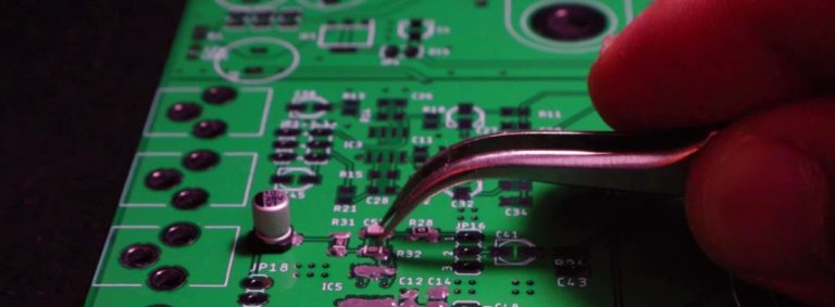
High-Frequency PCB Design Manufacturing
5G communication often involves higher frequency bands, including millimeter-wave frequencies. PCB designers must carefully manage signal integrity, impedance control, and minimize losses to ensure optimal signal transmission at these frequencies.
Antenna Integration
5G relies heavily on multiple antennas and MIMO (Multiple Input Multiple Output) technology for improved data throughput and connectivity. 5G PCBs must be designed to accommodate the placement, routing, and isolation of multiple antennas to optimize signal performance.
Thermal Management
The increased data handling and processing associated with 5G can result in higher power consumption. Effective thermal management strategies are crucial to prevent overheating and ensure long-term reliability of the PCB
EMI and RF Shielding
The use of higher frequency bands in 5G transmission increases the risk of electromagnetic interference (EMI). PCB designers must implement RF shielding and grounding techniques to minimize interference and maintain signal quality
Collaboration with RF PCB Design Engineers
Successful integration of 5G technology requires close collaboration between PCB designers and RF (Radio Frequency) engineers. This collaboration ensures that the PCB layout optimally supports the RF requirements for high-speed data transmission.
Simulation and PCB Testing
Advanced simulation tools and testing processes are vital to predict and validate the behavior of 5G signals within the PCB. This ensures that the design meets the performance expectations of 5G technology.
Future-Proofing
As 5G technology continues to evolve, PCB designers must consider scalability and future-proofing in their designs. This involves designing PCBs that can accommodate updates and changes as the technology matures.
Rise of 5G and transformative impact
Enhanced Mobile Connectivity: 5G is set to revolutionize the way we use mobile devices. With its faster data speeds and reduced latency, 5G will enable seamless streaming of high-definition content, facilitate faster downloads and uploads, and enhance online gaming experiences. Users will be able to access data-intensive applications and services with unprecedented speed and reliability.
Internet of Things (IoT) Advancement: The IoT ecosystem is expected to expand rapidly with the advent of 5G. The increased device connectivity and reduced latency of 5G will support the seamless integration of a vast number of IoT devices, enabling advanced applications in areas like smart homes, smart cities, industrial automation, and healthcare. 5G will provide a foundation for efficient communication and data exchange between interconnected devices, leading to improved automation, real-time monitoring, and process optimization.
Automotive Electronic: 5G technology will play a crucial role in the development and deployment of automotive electronic. The ultra-low latency of 5G networks allows for near-instantaneous communication between vehicles, infrastructure, and other connected devices. This high-speed, low-latency connectivity is essential for enabling advanced features like real-time navigation, vehicle-to-vehicle communication, and remote control capabilities.
Augmented and Virtual Reality: 5G can unlock the full potential of augmented reality (AR) and virtual reality (VR) applications. The combination of high data speeds and low latency offered by 5G networks will enable immersive and lag-free experiences in AR/VR environments. This has implications across industries such as gaming, entertainment, education, training, and remote collaboration.
Industry 4.0 and Smart Electronic: The Industrial Internet of Things (IIoT) and smart manufacturing will be significantly advanced by 5G. With the ability to handle a massive number of connected devices and machines in real-time, 5G networks will facilitate advanced automation, machine-to-machine communication, predictive maintenance, and real-time monitoring. This will lead to increased productivity, efficiency, and cost savings in industrial processes.
PCB Manufacturing Design For 5G Fundamental Goals
Enhanced Data Speeds: 5G aims to deliver significantly faster data speeds compared to previous generations. It uses advanced technologies like massive MIMO (Multiple-Input Multiple-Output) and higher frequency bands to achieve this. The increased data speeds enable faster downloading and uploading of data, smoother video streaming, and better overall network performance.
Reduced Latency: 5G strives to reduce latency, which is the delay in data transmission between devices. Lower latency is crucial for applications that require real-time communication and quick response times, such as autonomous vehicles, remote surgery, and virtual reality. By minimizing delays, 5G enables near-instantaneous communication and enhances user experience.
Increased Device Connectivity: 5G aims to connect a massive number of devices simultaneously. It utilizes technologies like network slicing and improved signaling efficiency to accommodate a high density of internet-connected devices. This connectivity is essential for the Internet of Things (IoT), where various devices communicate with each other and share data.
PCB Design Manufacturing Lead 5G connection
High-Frequency Design
5G networks operate at higher frequency bands compared to previous generations. PCBs need to be designed and manufactured to support these higher frequencies without signal degradation or loss. PCB design techniques like controlled impedance routing, transmission line optimization, and careful placement of components are essential to maintain signal integrity.
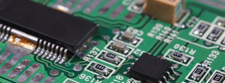
PCB Miniaturization and Integration
5G infrastructure requires a massive number of components, including antennas, RF filters, and amplifiers, to be integrated into a compact form factor. PCB design plays a crucial role in miniaturizing the overall size while integrating multiple functionalities on a single board. Advanced manufacturing techniques like high-density interconnect (HDI) and microvia technologies are employed to achieve miniaturization and component integration
PCB Thermal Management
5G networks generate significant heat due to high data rates and increased power consumption. Efficient thermal management is critical to maintain the performance and reliability of network components. PCB design should include proper thermal vias, thermal pads, and heat dissipation techniques to efficiently manage heat. Manufacturing techniques such as metal core PCBs or substrate materials with high thermal conductivity help improve thermal dissipation.
PCB RF Design and Antenna Integration
5G relies on multiple antennas and advanced RF components to achieve high-speed data transfer and low latency. PCB design enables the integration of antennas, RF filters, and amplifiers in close proximity, reducing signal losses and achieving optimal signal strength. Design techniques such as controlled impedance traces and specialized ground plane layouts are employed to ensure efficient RF performance.
PCB Material Selection
PCB material selection is critical for achieving high-speed and high-frequency performance in 5G applications. High-frequency laminates with low dielectric loss and stable electrical properties at high frequencies are used. Manufacturing processes should take into account the material properties to ensure consistent performance throughout the PCB.
In the context of 5G, high-Tg FR4 PCBs provide the thermal stability required for reliable operations in demanding environments. With higher glass transition temperature (Tg), these PCBs can withstand elevated temperatures without experiencing dimensional changes or performance degradation. This is especially important for high-power 5G devices that generate significant heat. The incorporation of high-Tg FR4 PCBs ensures effective thermal management, reducing the risk of signal loss or component failure due to excessive heat. By maintaining optimal performance in challenging thermal conditions, high Tg FR4 PCBs reinforce the infrastructure necessary for seamless 5G connectivity.
While high-Tg FR4 PCBs offer thermal stability and improved performance, they may come at a higher cost compared to standard FR4 materials. Manufacturers need to weigh the benefits and costs associated with different material options to ensure that the selected materials meet performance requirements while staying within PCB manufaturing costs constraints.
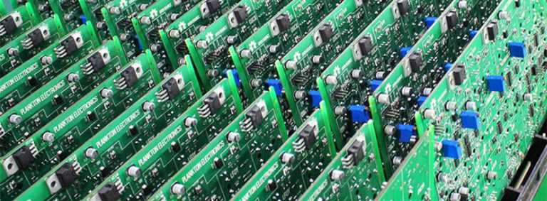
Manufacturing Efficiency
Rapid deployment of 5G networks requires efficient PCB manufacturing processes. Advanced techniques like automated manufacturing, surface mount technology (SMT), and automated optical inspection (AOI) improve manufacturing efficiency, reduce errors, and enable large-scale production of PCBs for 5G infrastructure.
Critical Role of PCB Design Manufacturing in 5G
The critical role of PCB design manufacturing in enabling 5G connectivity cannot be overstated. With the advent of 5G technology, the demand for faster and more reliable communication has soared, necessitating the development of advanced PCB solutions. Custom PCB fabrication, multilayer PCB fabrication, advanced PCB manufacturing techniques, and high-Tg FR4 PCBs have emerged as key contributors to the realization of 5G networks.
Custom PCB fabrication:
Custom PCB fabrication plays a pivotal role in tailoring circuit boards specifically for 5G applications. Designers can optimize the layout, component placement, and trace routing to accommodate the unique requirements of high-speed and high-frequency signals in 5G systems. By using custom fabrication processes, manufacturers can ensure precise manufacturing, resulting in improved signal integrity and overall performance. This level of customization is crucial in enabling the seamless operation of 5G networks.
Multilayer PCB fabrication:
Multilayer PCB fabrication offers a tremendous advantage for 5G connectivity. The complexity and density of electronic components in 5G systems demand higher integration capabilities. Multilayer PCBs allow for the incorporation of multiple signal and power layers into a single board, effectively utilizing space and facilitating the integration of various 5G components such as antennas, transceivers, RF filters, and power management circuits. This integration not only saves space but also enables reliable and high-performance connectivity essential for 5G networks.
Advanced PCB manufacturing:
Advanced PCB manufacturing techniques are indispensable in meeting the stringent requirements of 5G systems. Precise etching and drilling processes, fine-line and microvia technologies, and controlled impedance manufacturing ensure the accurate reproduction of intricate PCB designs with high routing density and impedance matching. These techniques are vital for the seamless transmission of high-frequency signals in 5G networks, reducing signal loss and maintaining low latency. Advanced manufacturing processes pave the way for efficient and effective 5G connectivity.
Conclusion
As 5G technology reshapes our digital landscape, PCB designers find themselves at the forefront of innovation. The integration of 5G in PCB design demands a deep understanding of high-frequency signal management, thermal considerations, and collaborative efforts with RF engineers. By addressing these challenges head-on and leveraging advanced design tools, PCB designers are shaping the future of connectivity, enabling a world of limitless possibilities.
PCB design manufacturing conquers 5G integration challenges by providing customized solutions that meet the unique requirements of 5G technology. It enables the precise layout, component placement, and trace routing necessary for high-speed and high-frequency signals.
With advanced manufacturing techniques, manufacturers can achieve accurate reproduction of intricate designs, ensuring optimal signal integrity and reducing signal loss. Multilayer PCB fabrication allows for higher integration and space utilization, accommodating various 5G components. Additionally, high-Tg FR4 PCBs provide thermal stability, allowing reliable operation in demanding environments. By leveraging these capabilities, PCB design manufacturing plays a crucial role in conquering the challenges and enabling seamless 5G integration.
In summary, PCB design manufacturing conquers 5G integration by ensuring signal integrity, supporting high-frequency requirements, enabling miniaturization and integration, facilitating antenna integration, managing thermal issues, and considering design for manufacturing aspects. These factors collectively contribute to the seamless integration of 5G technology in various devices and network infrastructures.