
The Benefits of High-density SMT Chip Processing for Circuit Boards

The development path of SMT proofing and small batch processing has developed rapidly towards the direction of high density. With the development of electronic technology, the market also requires more miniaturization and precision of electronic products. Nowadays, the technology of SMT chip processing is more and more widely used in the electronic industry. In order to realize the miniaturization of electronic products, make them thinner and lighter, and have more versatility, the requirements for the design of circuit boards is now required. More and more strict, the technical requirements are getting higher and higher.
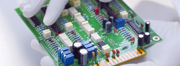
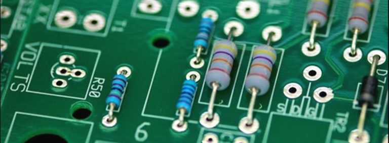
The assembly of SMT chip processing has high relative density, lightweight, and lightweight electronic components. The volume and total weight of chip components are only about 1/10 of those of traditional plug-in components. Usually, after SMT is selected, the volume of electronic components is 40%~60% smaller, and the total weight is reduced by 60%~80%. High reliability and strong anti-vibration capability. The spot welding defect rate is low. Good high-frequency performance. Electromagnetic and radio frequency interference is reduced. It is easy to realize automation technology and improve productivity. Control costs can reach 30% to 50%. Save raw materials, electrical energy, machinery and equipment, human resources, and time. The benefits of high-density SMT chip proofing processing are numerous, and many electronic OEM processing orders are processed by high-density chip processing.
The benefits of high-density SMT chip processing:
1. The micro-hole has a low aspect ratio, and the signal transmission reliability is higher than that of the general through-hole.
2. Micro holes can improve the flexibility of circuit configuration and make circuit design easier.
3. The use of high-density patches for the same electronic product scheme can reduce the size of the pcba circuit board and thus reduce the cost.
Fourth, the design of high-density SMT chip processing can choose a thinner dielectric and lower potential inductance in the structure.
5. The use of micro-hole interconnection can shorten the contact distance, reduce signal reflection and crosstalk between lines, and the components can have better electrical properties and signal accuracy.
6. Increase the wiring density and increase the line capacity per unit area with micro-hole thin lines, which can meet the assembly requirements of high-density contact components, and is conducive to the use of advanced construction.
7. Micro-via technology allows the carrier board design to shorten the distance between grounding and signal layers, thereby improving RF/electromagnetic wave/electrostatic discharge (RFI/EMI/ESD) interference. The number of grounding wires can be increased to prevent damage to components caused by instantaneous discharge due to static electricity accumulation.