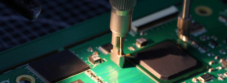

The Methods of Reducing Noise and Electromagnetic Interference in PCB

Nowadays, the sensitivity of electronic equipment is getting higher and higher, which requires the equipment to have a stronger anti-interference ability. Therefore, in the PCB design, how to improve the Interference in PCB Board has become a key issue of the circuit board project. Therefore, methods to reduce noise and electromagnetic interference in PCB design:
1. If you can use low-speed chips, don’t use high-speed chips.
2. Use a resistor in series to reduce the speed of the control circuit.
3. Use the lowest frequency clock that meets the system requirements.
4. The clock generator is as close as possible to the device using the clock.
5. Enclose the clock area with a ground wire and keep the clock wire as short as possible.
6. The printed circuit board should try to use 45-degree fold lines instead of 90-fold lines to reduce the external emission and coupling of high-frequency signals.
7. The printed board is partitioned according to frequency and current switching characteristics, and noise components and non-noise components should be separated further.
8. Keep the clock, bus, and chip selection signals away from I/O lines and connectors.
9. The analog voltage input line and reference voltage terminal should be as far away as possible from the digital circuit signal line.
10. The component pins should be as short as possible, and the decoupling capacitor pins should be as short as possible.
11. The key line should be as thick as possible, and protective ground should be added on both sides. The high-speed line should be short and straight.
12. Do not parallel lines sensitive to noise with high-current, high-speed switching lines.
13. Do not route wires under the quartz crystal and under noise-sensitive devices.
14. For weak signal circuits, do not form current loops around low-frequency circuits.
15. Do not form a loop in the signal. If it is unavoidable, make the loop area as small as possible.