
How to Layout LED Switching Power Supply PCB Components?
With the development of science and technology, LED technology is also constantly developing, bringing all kinds of convenience to our lives, providing us with all kinds of life information, and benefiting us human beings. If you want the LED switching power supply to have the best PCB components layout, then before proceeding with component layout design, the first thing you need to do is to fully consider the size of the PCB board.
When the PCB size in the switching power supply is too large, the printed lines are too long, which will increase the impedance and reduce the noise resistance, and the cost will increase accordingly. Once the printed circuit board is too small, heat dissipation is not good, and adjacent lines are easily disturbed. Generally speaking, the best shape of the PCB circuit board for LED switching power supply is a rectangle with an aspect ratio of 3:2 or 4:3. The components located on the edge of the Electronic circuit board are generally not less than 2mm from the edge of the circuit board.
After completing the design of the PCB prototype size, we also need to consider the problem of distributed parameters between components, which is especially important for circuits that work under high-frequency conditions. Generally, the LED circuit should be arranged in parallel as much as possible, so that it is not only beautiful, but also easy to install and solder, and easy to mass produce.

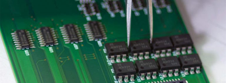
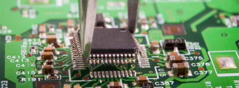
When placing the components of the PCB manufacturing, do not blindly ask for speed. At this time, you need to comprehensively consider future soldering issues. This also requires engineers to reasonably lay out the components, and don’t put the components too densely. In the design process, the engineer should center on the core components of each functional circuit and carry out the overall component layout around the core components. In the layout process, the components should be evenly, neatly, and compactly arranged on the Electronic PCB, and the leads and connections between the components should be reduced and shortened as much as possible. The decoupling capacitor should be as close as possible to the VCC of the device.
In addition, when performing the PCB layout of the LED switching power supply, it is recommended that engineers arrange the position of each functional circuit unit according to the circuit flow. This layout can make the signal flow more effective and fast, and keep the signal as possible Consistent direction. In the layout of the PCB board, the first principle is to ensure the layout rate of the wiring, pay attention to the connection of the flying lines when moving the components, and put the components with the connection relationship together. Reduce the loop area as much as possible to suppress the radiation interference of the switching power supply. Today’s LED lights may have some problems, but we believe that with the rapid development of science and technology, these problems will eventually be solved with the efforts of our scientific researchers. The future LEDs must be high-efficiency and high-quality.