What Should be Paid Attention to When Welding Double-Sided Circuit Boards?

In order to ensure the reliable conduction effect of the double-sided circuit, the connecting holes on the board should be welded with wires first, and the protruding part of the connecting wire tip should be cut to avoid hurting the operator’s hand. This is the board connection preparation. So, what issues should be paid attention to when welding double-sided circuit boards?
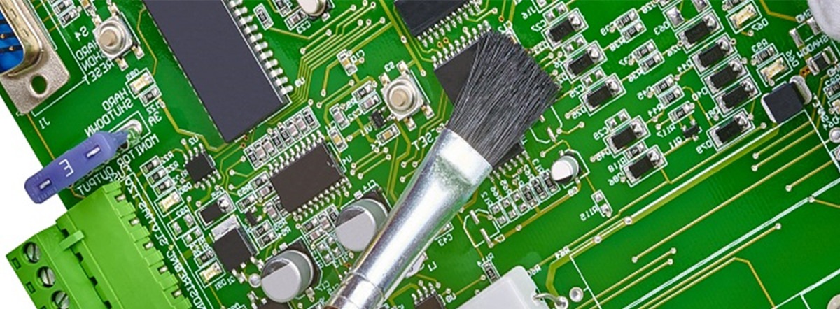
Compared with the single-sided circuit board, the wiring density of the double-sided circuit board becomes larger and the aperture is smaller. The metalized holes on which the layer-to-layer interconnection relies are directly related to the reliability of the printed circuit board. As the pore size shrinks, some debris, such as brush debris, ash, etc., once remaining in the small hole, will make electroless copper and electroplating useless.
1. For devices that require shaping, they should be shaped first and then plug-in according to the requirements of the process drawings.
2. After shaping, the model side of the diode should face up, and there should be no discrepancies in the length of the two pins.
3. When inserting devices with polarity requirements, pay attention to their polarity not being reversed. After inserting, no matter whether it is a vertical or horizontal device, there must be no obvious tilt.
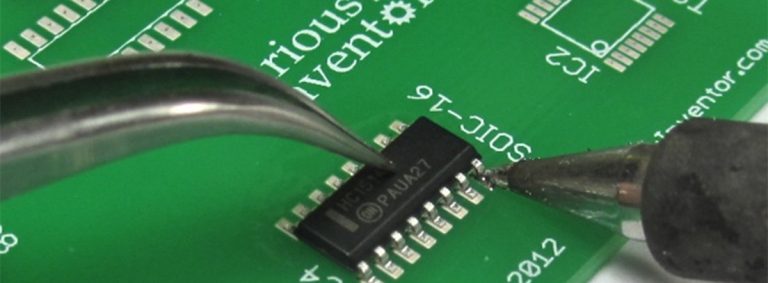
4. The power of the soldering iron used for novation circuit board welding is between 25~40W, the temperature of the soldering iron tip should be controlled at about 242℃, and the soldering time should be controlled at 3~4 seconds.
5. When the led PCB board is soldered, it is generally operated according to the welding principle of the device from short to high, from the inside to the outside. The welding time must be mastered. If the time is too long, the device will be burnt, and the copper line on the copper-clad board will also be burnt.
6. Because it is a double-sided soldering circuit board, a process framework for placing the circuit board should also be made, so as not to squeeze the components underneath.
7. After the SMD PCB board is soldered, a comprehensive inspection should be carried out to find out where there are missing soldering holes, and after confirmation, trim the excess device pins, and then flow into the next process.
8. The specific operation should also strictly follow the relevant process standards to ensure the quality of metal core PCB welding.

