
What Are The Advantages of Full Turnkey PCB Assembly Service
Experience hassle-free PCB manufacturing with our Full Turnkey PCB Assembly Service. We handle it all – from design to delivery, component sourcing to rigorous testing. Streamline your production process and accelerate time-to-market with our comprehensive solution.” 1. Assembly Type: FR4, FPC, Rigid-flex PCB, Metal base PCB. 2. Assembly Specification: Min size L50″W50mm; Max size: L510*460mm 3. Assembly thickness: Min thickness: 0.2mm; Max thickness: 3.0mm Components DIP: 01005Chip/0.35 Pitch BGA Minimum device accurace: +/-0.04mm Minimum footprint distance: 0.3mm 4. Components Specification Components DIP: 01005Chip/0.35 Pitch BGA Minimum device accuracy: +/-0.04mm Minimum footprint distance: 0.3mm 5. File format: BOM list; PCB Gerber file: Click the PCBA capability in this link Get our categary
Description
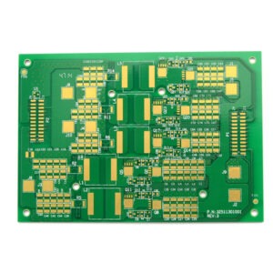
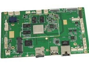
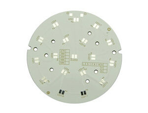
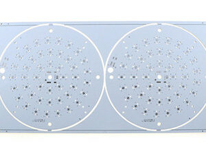
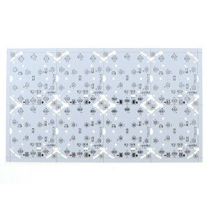
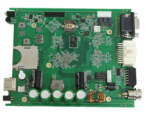
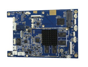
 PCB Assembly for DVB Mainboard | 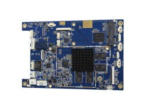 PCB Assembly for Game Machine Board | 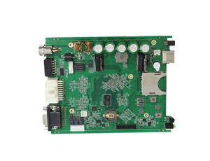 PCB Assembly for Communication Board |
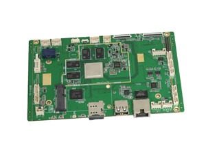 PCB Assembly for Signal Processing Board | 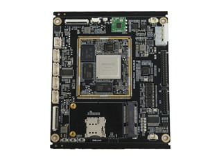 PCB Assembly for Gamera Motherboard | 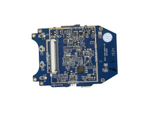 PCB Assembly for Portable Device Board |
Full TurnKey PCB Assembly:
Full Turnkey PCB Assembly Service is a comprehensive solution offered by electronics manufacturing service providers to manage the entire production process of printed circuit boards (PCBs), from the initial concept to the final product delivery. Full TurnKey covers all aspects of PCB fabrication and assembly, including PCB design, manufacture of PCBs, electronic parts procurement, tracking of orders, quality inspections, and final PCB assembly, electronic testing, PCB and assembly quality control, and packaging, among others.
PCBA assembly contract means that customers provide a full set of information in PCB Gerber file, PCBA manufacturers provide electronic components procurement, PCB manufacturing processing, SMT, DIP plug-in and PCBA testing one-stop electronic manufacturing services.
The electronic processing mode of PCBA circuit board assembly, let the enterprises be free from the electronic manufacturing process, save the PCB manufacturing costs in electronic material procurement, warehousing, outsourcing, logistics and personnel, and the one-stop PCBA circuit board assembly mode has actually become the mainstream trend of electronic processing. Therefore, the development of advantages of PCBA circuit board assembly contract processing enterprises will come in handy, because it perfectly solves the problems faced by traditional PCBa production and processing process management. So, what are the advantages of Full Turnkey PCB Assembly Service?
This comprehensive service is particularly valuable for businesses seeking a one-stop solution for their PCB manufacturing needs,let’s delve into each process involved in Full Turnkey PCB Assembly Service in more detail:
1. Professional PCB Design Service Team:
- Collaborative Design Review: The service provider works closely with the customer to review and refine the PCB design. This involves checking for design errors, ensuring proper component placement, and optimizing the layout for manufacturing efficiency.
- Design Validation: Rigorous validation processes are employed to ensure that the design meets all functional and performance requirements. This can involve simulations, design rule checks (DRC), and design for manufacturability (DFM) analysis.
PCB Schematic Design: We can help you create or review schematic diagrams, review your PCB designs to identify potential issues, recommend design improvements, and ensure they adhere to best practices for manufacturability and functionality. ensuring accurate and reliable connections between components. This stage is critical for defining the electrical behavior of your PCB.
PCB Layout and Routing: Our team can assist with PCB layout and routing, optimizing component placement, trace routing, and ensuring signal integrity. This includes considerations for high-speed and high-frequency circuits.
Electronic Component Selection: We can provide recommendations for component selection based on your project’s requirements, including considerations for cost, availability, and performance.
PCB Stackup Design: For multilayer PCBs, we can help you design an appropriate layer stackup, considering factors such as impedance control, signal integrity, and thermal management.
Signal Integrity Analysis: Our team can perform signal integrity analysis to ensure that high-speed signals maintain their integrity throughout the PCB, minimizing signal degradation and noise.
Power Integrity Analysis: We can assess the power distribution network to ensure stable and efficient power delivery to all components, reducing the risk of voltage drops or noise.
Thermal Management: We can provide guidance on thermal management strategies to prevent overheating and ensure the reliability of your PCB, especially in applications with high-power components.
EMI/EMC Compliance: Our engineers can help design your PCB to meet electromagnetic interference (EMI) and electromagnetic compatibility (EMC) standards, reducing the risk of interference and ensuring compliance.
PCB Design for Manufacturability (DFM): We can assist in designing PCBs that are manufacturable, taking into account factors such as component placement, soldering, and assembly techniques.
PCB Prototyping Support: We can guide you through the prototyping phase, helping with component sourcing, assembly, and testing to ensure your design functions as expected.
PCB Design for Testing (DFT): We can help you design PCBs that are easy to test and troubleshoot, reducing testing time and costs during production.
PCB Manufacturing Costs Optimization: We can provide cost-effective design solutions by optimizing component choices, reducing waste, and considering cost-efficient manufacturing techniques.
Customized PCB Solutions: Our team can tailor our services to your specific project needs, whether it’s a single-layer PCB, double-layer PCB, Rigid-Flex PCB Design, High-Frequency PCB Design,High-Precision PCB Design,High-Density PCB Design, or a complex, multilayer PCB design, Blind Buried PCB Design, We adhere to the “customer orientation” and focus on providing customers with reasonable solutions for product performance, cost and manufacturing cycle.
2. Electronic Component Procurement
The full turnkey PCB assembly service manufacture have series of resistors and capacitors and common inductances, magnetic beads. connectors, crystal oscillators, diode triode, and provide full BOM component supporting services for research and development.
- Vendor Selection: This service provider selects reputable electronic component suppliers based on factors like reliability, availability, and cost-effectiveness, they will provide supplier names and part numbers for each component, they can help negotiate with suppliers to secure favorable terms and pricing for your components, and choose reliable suppliers based on factors such as cost, quality, and lead times.
- Component Sourcing: The one-stop PCB assembly supplier sources all required components, including semiconductors, resistors, capacitors, connectors, and more. This may include handling hard-to-find or obsolete parts. They will create a comprehensive BOM list based on your PCB design, including detailed specifications for each component.
Components will be categorized based on type (e.g., resistors, capacitors, ICs) and purpose (e.g., power, signal processing). They also specify the quantity of each component required for your project, and identify the lifecycle status of each component (active, end-of-life, obsolete) to ensure long-term availability, suggest alternative components or sources for components with limited availability.
- Inventory Management: Efficient management of component inventory to ensure that shortages or delays are minimized during production.
3. In-house PCB Fabrication:
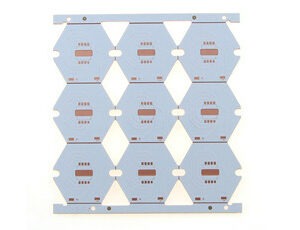
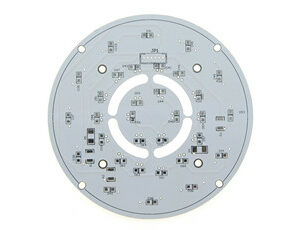
- PCB Material Selection: Choosing the appropriate PCB substrate material to different PCB projects requests, such as normal FR4 PCB, high tg FR4 PCB, Rogers PCB, Isola PCB, or aluminum core PCB, metal core PCB, Flexible PCB, based on the project’s material and function requirements.
- Fabrication Oversight: Managing the entire PCB fabrication process, including the creation of PCB panels, layer stacking, and ensuring that manufacturing standards are met.
- Control Over Quality: In-house fabrication allows for strict control over the entire manufacturing process. Quality control measures can be implemented at every stage to ensure that PCBs meet design specifications and industry standards.
- Reduced Lead Times: By eliminating the time needed for shipping and coordination with external manufacturers, in-house fabrication can significantly reduce lead times. This is especially advantageous for projects with tight deadlines. In-house fabrication facilitates rapid iterations and design changes. This is particularly valuable for projects that require quick adjustments and testing.
- Cost Savings: Over the long term, in-house PCB fabrication can lead to cost savings. While there are initial equipment and infrastructure investments, the elimination of external manufacturing costs can be cost-effective for high-volume or long-term production needs.
- Customization and Prototyping: In-house fabrication offers flexibility for customization and prototyping. Design changes and small production runs can be accommodated more readily without the need to meet minimum order quantities (MOQs) imposed by external manufacturers.
- IP Protection: Keeping the fabrication process in-house can enhance intellectual property (IP) protection. There’s less risk of designs being exposed to third-party manufacturers, which can be important for proprietary or sensitive projects. By controlling the entire process internally, you can implement security measures to safeguard sensitive design data and intellectual property.
- Reduced Communication Overheads: In-house fabrication reduces the need for extensive communication and coordination with external manufacturers, which can sometimes lead to misunderstandings or errors in the manufacturing process. Any issues that arise during the fabrication process can be addressed promptly, reducing the risk of production delays.
- Prototyping and Research: For research and development purposes, in-house fabrication allows for easy experimentation and testing of new PCB designs without external dependencies.
4. In-house PCB Assembly:
Advances in electronic technology have brought more possibilities to PCB assembly. There are now three commonly used assembly technologies, one is SMT (surface mount technology), the second is THT(through hole technology), and the third is a combination of the first two.
To assemble highly complex circuits, it is difficult to achieve the desired effect using only SMD or THT, and we need to combine SMT and THT technologies. The one-stop full turnkey PCB assembly service offers a combination of both technologies.
The entire process of PCBA processing requires SMT mounters, reflow soldering, wave soldering, and other precision processing equipment and various testing equipment, such as X-ray, 3DAOI,SPI, intelligent first article tester, BGA rework station, etc. and so on. Perfect SMT processing line equipment plays an important role in production control, production delivery, cost control, project property security, production flexibility, material supply chain management, and production efficiency.
Advantages of SMT
- High Component Density: SMT allows for higher component density on PCBs, reducing board size and weight.
- Enhanced Performance: Smaller components and shorter trace lengths can improve electrical performance and signal integrity.
- Automation: SMT can be highly automated, leading to consistent, high-precision assembly and reduced labor costs.
- Miniaturization: SMT enables the use of smaller, more lightweight components, ideal for portable and miniaturized devices.
- Cost Efficiency: Reduced material waste and lower assembly costs are often associated with SMT manufacturing.
Through-Hole Technology (THT):
Careful insertion and soldering of through-hole components where applicable. Through-Hole Technology (THT) is a method of electronic component assembly on printed circuit boards (PCBs) that involves inserting component leads through holes drilled in the PCB and then soldering them to the opposite side to establish electrical connections. THT has been widely used in electronics manufacturing for decades and remains relevant for various applications.
Advantages of THT
- Mechanical Strength: THT components are mechanically secured to the PCB through holes and solder joints, making them resistant to mechanical stress, vibration, and shock.
- High-Power Applications: THT components are suitable for high-power and high-current applications due to their robust mechanical connections and larger size.
- Reliability: THT solder joints are typically larger and more forgiving of variations in the soldering process, resulting in reliable connections.
- Repairability: THT assemblies are generally easier to repair or modify because components can be desoldered more readily than SMT components.
- Availability: Many electronic components are still available in THT packages, making THT assembly a viable choice for certain applications.
PCB Assembly Quality Assurance
Control Over Production: Having an in-house SMT line allows for direct control over the entire production process, from component placement to reflow soldering. This control enhances product quality and consistency. Continuous monitoring and inspection of the assembly process to identify and rectify any defects or issues. Comprehensive checks to ensure that all components are properly soldered, and the PCB meets industry standards and customer specifications.
- Inspection: Automated optical inspection (AOI) and X-ray inspection are commonly used to check for defects such as misalignment, solder bridges, or missing components. These inspections ensure the quality and reliability of the assembly. Visual inspection and testing are essential to ensure that the solder joints are properly formed and there are no solder bridges or cold joints. Automated inspection machines and manual checks are commonly used for quality control.
- Test: normally there are several test steps for PCB assebly line processing
IQC: Incoming inspection
IPQC: Production inspection; first ICR test
Visual QC: Regularly quality inspection
SPI test : Automatic solder paste optical inspection
AOI: SMD component welding detection, components shortage & component polarity detection
X-Ray: BGA test; QFN and other precision devices hidden PAD device inspection
Function test: Test function and performance according to customer’s test procedures and steps, Rigorous functional testing to verify that the assembled PCBs operate as intended.
Reworking: BGA rework equipment
Compliance Verification: Ensuring that the PCB assembly adheres to industry regulations and standards, such as IPC-A-610 for electronic assemblies.
Consider PCB Packaging and Shipping:
- Secure Packaging: Careful packaging to protect the finished PCBs during transit, minimizing the risk of damage. PCBs are sensitive to electrostatic discharge (ESD). They should be handled in ESD-safe environments and placed in antistatic bags to protect against static electricity.If there are components mounted on the PCB, they should be adequately protected. Components can be covered with foam or bubble wrap to prevent damage during shipping. When stacking PCBs for shipping, it’s essential to provide proper cushioning between each layer. Foam or cardboard dividers can be used to prevent PCBs from contacting each other.
- Shipping Logistics: Efficient logistical planning to ensure on-time delivery to the customer’s location, whether it’s a single prototype or a large production run. Vacuum packaging makes the circuit board tightly fixed, which can prevent friction, oxidation, dust and moisture, to ensure that the intact performance of the circuit board is maintained during transportation. Choose a reliable shipping method appropriate for your PCBs’ size, weight, and destination. Common options include courier services, air freight, and sea freight.
7. PCB Project Management:
- Coordination: Coordinating all stages of production, from PCB design, PCB fabrication, PCB assembly, electricity test to delivery, to ensure that the project progresses smoothly. Collaborate with the client or internal team to understand the PCB design requirements, specifications, and functionality needed, Offer design consultation and optimization to ensure the design is manufacturable and efficient.
- PCB Prototyping: Create a prototype of the PCB design for testing and validation, Create a prototype of the PCB design for testing and validation.
- PCB Manufacturing: Use in-house facilities to manufacture the PCBs, following industry best practices and quality standards.
- Assembly and Soldering: Assemble the electronic components onto the PCB using automated pick-and-place machines and soldering equipment. Ensure proper soldering techniques to avoid solder defects, such as cold joints or bridging. Utilize surface mount technology (SMT) and through-hole technology (THT) based on the design requirements.
- Single Point of Contact: Serving as a single point of contact for the customer, facilitating communication and issue resolution. Offer ongoing customer support to address any issues or concerns that arise after the PCB assembly process. Assist with debugging, troubleshooting, and further optimization if required.
Each step in the Full Turnkey PCB Assembly Service is meticulously managed to deliver high-quality PCBs that meet design specifications and industry standards. This comprehensive approach simplifies the manufacturing process for customers, enabling them to focus on their core business activities while ensuring a streamlined and efficient production cycle.
Full Turnkey PCB Assembly Application:
There are countless applications of PCBA in computer industry. The mother board, Graphics Processing Unit (GPU), Central Processing Unit (CPU), RAM, ROM, SD-Cards, SDRAM, DDR1,2,3,4, EEPROM, microcontroller boards, keyboard, computer mouse, gaming mouse, LED screen, laptops, tablets, notebook, etc..
At present, Finest PCB has accumulated rich experience in the high-tech PCB manufacturing industry for 20 years old. It can conduct comprehensive review, evaluation and suggestion for GERBER file and BOM lists, minimize smt PCB prototype cost and produce more reliable PCB products. offer fast quick turn one-stop PCB and assembly service. Here is the delivery time for our PCB assembly process below:
| Delivery Time | |
| Normal delivery time: | 24 hours( fastest 12 hours quick-turn) |
| Small production: | 72 hours( fastest 24 hours quick-turn) |
| Medium production: | 5 working days. |