
What are the 9 P Advantages of Multi-layer PCB and Single-sided or Double-sided PCB?

These intricate circuit boards boast a multitude of advantages that cater to the ever-evolving demands of the electronics industry. In this article, we delve into the distinct Advantages of Multi-layer PCB as preferred choice for a wide range of applications. In the dynamic landscape of modern electronics, the design and composition of printed circuit boards (PCBs) have witnessed remarkable advancements. One such innovation that has revolutionized electronic manufacturing is the advent of multi-layer PCBs.
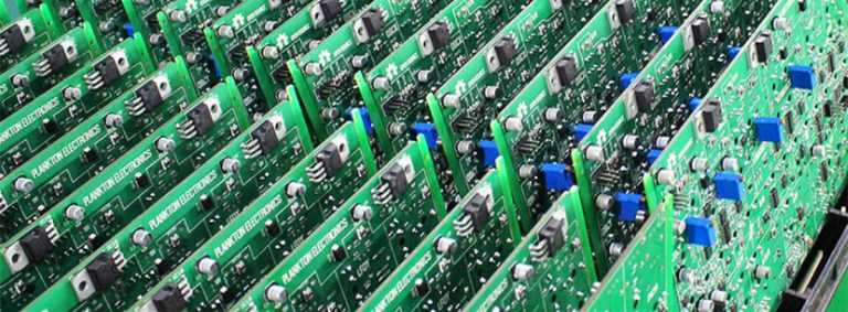
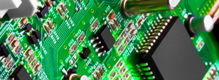
Multilayer circuit boards are actually formed by laminating and bonding several etched single or double panels. So, what are the Advantages of Multi-layer PCB compared with single-layer circuit boards and double-layer circuit boards? Let me share it with you below.
What is multi-layer PCB?
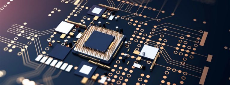
A multi-layer PCB (printed circuit board) is a type of circuit board that consists of multiple layers of conductive traces, insulating material, and often additional components. Unlike single-layer or double-layer PCBs, which have conductive traces on only one or two sides respectively, multi-layer PCBs have conductive traces on multiple layers stacked atop each other.
These layers are interconnected through vias, which are small plated holes that allow signals and power to pass between different layers. The inner layers are usually dedicated to signal routing, power planes, and ground connections. The outer layers typically host components, allowing for a higher density of components and more complex circuitry in a smaller space
The multiple layers in a multi-layer PCB provide several advantages, including improved signal integrity, reduced electromagnetic interference (EMI), enhanced thermal management, and greater design flexibility. Multi-layer PCBs are widely used in modern electronic devices that require compact size, high-performance, and reliability, such as smartphones, computers, automotive electronics, and medical devices.
Detail Advantages of Multi-layer PCB
Advantages 1: Enhanced Signal Integrity
One of the primary advantages of multi-layer PCBs is their ability to optimize signal integrity. These boards consist of multiple layers of copper traces separated by insulating materials, allowing designers to meticulously route signal traces while minimizing interference. This configuration drastically reduces the risk of signal loss, cross-talk, and electromagnetic interference (EMI), resulting in improved overall performance and reliability of the electronic device.
Miniaturization not only brings physical advantages in terms of PCB size and weight, but it also improves the signal integrity of electronic devices. As components are made smaller, the distance between them decreases, leading to reduced signal degradation and improved performance. This is particularly important in high-frequency applications, such as wireless communication and data transmission.
Advantages 2: Size and Weight Reduction
One of the most obvious advantages of miniaturization is the reduction in size and weight of electronic devices. Gone are the days of carrying around bulky laptops or struggling to fit a large television into a small living room. Miniaturization has allowed us to enjoy the benefits of technology without sacrificing convenience or aesthetics. Today, we can effortlessly slip a sleek tablet into our bags or mount a slim television on the wall, creating a minimalist and modern environment.
Modern electronic devices demand compactness without compromising on functionality. Multi-layer PCBs excel in this aspect by accommodating complex circuits in a smaller footprint. With the ability to stack numerous layers vertically, these PCBs enable designers to achieve high-density interconnections, accommodating more components and functionality within a limited space. This is particularly advantageous in applications such as smartphones, wearables, and IoT devices.
For portable devices and space-constrained applications, multi-layer PCBs offer a crucial advantage. By consolidating components into a smaller area, they contribute to reduced device size and weight, enhancing overall portability and design aesthetics.
Advantages 3: Power Distribution and Thermal Management
Another advantage of miniaturization in electronics is improved power distribution. By reducing the size of electronic components, it becomes easier to design and implement efficient power management systems. Smaller components have lower power requirements, resulting in reduced energy consumption and longer battery life.
Consider the evolution of laptops. In the past, laptops were notorious for their short battery life, often lasting only a few hours before needing to be recharged. However, with advancements in miniaturization, laptops have become more power-efficient, allowing us to work or play on the go without constantly worrying about finding an available power outlet. This has transformed the way we work and travel, providing us with the freedom and flexibility to be productive wherever we go.
Efficient power distribution and heat dissipation are critical for maintaining the longevity and stability of electronic components. Multi-layer PCBs facilitate the integration of power planes, providing dedicated layers for power and ground connections. This enhances the power integrity of the system, reduces voltage drops, and minimizes the risk of thermal issues. Additionally, the multiple layers act as effective heat sinks, dispersing heat generated by active components and optimizing thermal management.
Advantages 4: Complex PCB Design Support
Modern electronics often require intricate, densely packed designs. Multi-layer PCBs accommodate these complex designs more effectively than single or double-layer counterparts. Their flexibility in routing and component placement allows for the integration of advanced features and functionalities.
The design flexibility offered by multi-layer PCBs is unparalleled. Designers can route complex circuits with varying signal speeds, impedance requirements, and power needs, all within the same board. This flexibility fosters innovation and enables the creation of intricate electronic systems that meet specific performance criteria. Moreover, multi-layer PCBs can incorporate both surface-mount and through-hole components, accommodating a diverse range of components and technologies.
PCB design techniques like controlled impedance routing, transmission line optimization, miniaturization and Integration, If you want to integrate more PCB solutions, multi-layer PCBs play an important role, Especially with the advent of the 5G technology, that is why PCB Design Manufacturing Conquer 5G Integration.
Advantages 5: Reduced Electromagnetic Emissions
Electromagnetic emissions can lead to interference with other electronic devices and even pose health risks. Multi-layer PCBs, with their optimized signal routing and reduced EMI, contribute to electromagnetic compatibility (EMC). By suppressing unwanted radiation and minimizing susceptibility to external electromagnetic fields, these boards help ensure that electronic devices comply with stringent EMC standards.
Advantages 6: Reduced Noise and Crosstalk
Multi-layer PCBs are adept at minimizing noise and crosstalk between signal traces. With dedicated ground and power planes, electromagnetic interference is reduced, resulting in cleaner signals and less interference between components.
Advantages 7: Easier Troubleshooting and Maintenance
Miniaturization has made troubleshooting and maintenance of electronic devices easier and more efficient. With smaller and more modular components, it becomes easier to identify and replace faulty parts, reducing downtime and repair costs.
Advantages 8: PCB manufacturing Costs Effective
Contrary to what one might expect, miniaturization has also led to cost-effectiveness in the production of electronic devices. While the initial investment in research and development may be significant, the economies of scale achieved through mass production of smaller components result in lower manufacturing costs.
While multi-layer PCBs may seem more complex, they often offer cost savings in the long run. Their ability to reduce the number of external electronic components, such as connectors and cables, can lower PCB manufacturing costs and PCB assembly costs. Moreover, their reliability minimizes maintenance and repair expenses.
Advantages 9:Enhanced Electronic Component Density
One of the primary advantages of multi-layer PCBs is their ability to pack a substantial number of components into a compact space. Unlike single-layer or double-layer PCBs, which have limitations in component placement, multi-layer PCBs offer multiple layers of interconnection. This means more components can be added without increasing the PCB’s physical size.
With each new generation of devices, we demand more functionality, more power, and more features. This often means adding more electronic components to the PCB. But where do you put them all? Once again, multi-layer PCBs come to the rescue.
By adding more layers, you can increase the number of components that can be mounted on the board. This means you can add more functionality and complexity to your device without increasing its size. It’s like adding more rooms to your house—you can have a kitchen, a living room, a home theater, and a games room, all without expanding the footprint of your house.
Single-Sided PCBs with Economical Solution
Single-sided PCB, the most basic design available. As the name suggests, these boards have conductive material on only one side. With a straightforward design and fewer components than their double-sided or multi-layer counterparts, single-sided PCBs are the most cost-effective solution for simple electronic applications.
However, their simplicity may also be their downfall for complex devices. The lack of a second conductive layer means that the circuit paths cannot cross. This limits the complexity of the device it can power. Single-sided PCBs also lack the durability of their more layered counterparts, making them unsuitable for heavy-duty applications.
Advantates of Double-sided PCBs
Double-sided PCBs are the go-to choice for a wide range of applications, from traffic lights and HVAC systems to amplifiers and vending machines. They offer a higher circuit density than single-sided boards, allowing for more complex designs without significantly increasing the size of the board.
While they are slightly more expensive than single-sided PCBs, the versatility of double-sided boards makes them a cost-effective solution for many applications. That said, the design and manufacturing process can be more complex, requiring careful planning to ensure that the circuit paths do not interfere with each other. Double-sided PCBs offer a good balance of cost, complexity and performance for many commercial electronics.
Multi-layer PCBs compare with Single and Double-layer PCBs
1. Multilayer circuit boards have high assembly density and small size; as the volume of electronic products becomes smaller and smaller, the demand for multilayer circuit boards is also increasing.
2. The multi-layer PCB board is convenient for wiring, the wiring length is greatly shortened, and the connection between components is shortened, thereby increasing the speed of signal transmission.
3. For high-frequency circuits, after adding the ground layer, the signal line will form a constant low impedance to the ground layer, the circuit impedance is greatly reduced, and the shielding effect is better.
4. For electronic products with high heat dissipation function requirements, multilayer circuit boards can be provided with a metal core heat dissipation layer, which is convenient to meet the needs of special functions such as shielding and heat dissipation.

In terms of performance, multi-layer Integrated circuit boards are better than Single-sided or Double-sided PCB, but the higher the number of layers, the greater the production cost, the relatively long processing time, and the more complicated quality inspection.
What are the common multi-layer PCB
The most common multi-layer Electronic circuit board is the four- or six-layer board. The difference between the four-layer board and the six-layer board is that there are two more internal signal layers between the middle layer, the ground layer, and the power layer. The six-layer board is more than the four-layer board. The laminate should be thicker. Single and double-layer boards are easy to distinguish. Hold the board and look at the light. Except for the wiring on both sides, the rest is transparent. But for the four-layer board and the six-layer board, if there is no corresponding mark on the board, it is not so easy to make a simple distinction.
Conclusion
In conclusion, multi-layer PCBs are at the forefront of modern electronics design for numerous reasons. Their ability to boost component density, enhance signal integrity, and support complex designs makes them a valuable asset in various industries, from consumer electronics to aerospace and beyond. As technology continues to advance, multi-layer PCBs are poised to remain a crucial element in the evolution of electronic devices.
Generally speaking, High-density multi-layer circuit boards have been widely used in the manufacture of electronic products due to their design flexibility, economic superiority, stable electrical performance, and reliability.