What is the Difference Between HDI Board and PCB Board?
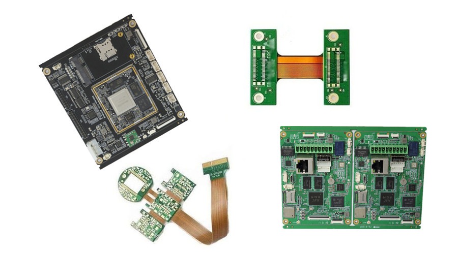
HDI board (High-Density Interconnector), namely a high-density interconnection board, is a circuit board with a relatively high line distribution density using micro-blind and buried via technology. The HDI board has an inner layer circuit and an outer layer circuit, and then uses processes such as drilling and metallization in the hole to realize the internal connection of each layer of the circuit.
PCB (Printed Circuit Board), the Chinese name for printed circuit board, is also known as a printed circuit board. It is an important electronic component, supports electronic components, and is a carrier for the electrical connection of electronic components. Because it is made by electronic printing, it is called a “printed” circuit board.
HDI boards are generally manufactured by a layer-by-layer method, and the more the number of layers, the higher the technical grade of the plate. Ordinary HDI boards are basically layered once, and high-end HDI uses layering technology of 2 or more times. At the same time, advanced technologies such as stacking holes, electroplating and filling holes, and laser direct drilling are used.
When the density of the PCB increases beyond the eight-layer board, it is manufactured with HDI, and its cost will be lower than that of the traditional and complex pressing process. HDI board is conducive to the use of advanced packaging technology, and its electrical performance and signal accuracy are higher than traditional PCBs. In addition, HDI boards have better improvements in radio frequency interference, electromagnetic wave interference, electrostatic discharge, and heat conduction.


