
PCB Board Production Manufacturing Process

The production process of PCB board is relatively complex, and it involves a wide range of processes, from simple mechanical processing to complex mechanical processing, common chemical reactions, photochemical, electrochemical, thermochemical, and other processes, computer-aided design CAM, and many other aspects of knowledge. Because the production process is a non-continuous assembly line form, any problem in any link will cause the entire line to stop production. Or as a result of a large number of scraps, if printed circuit boards are scrapped, they cannot be recycled and reused.
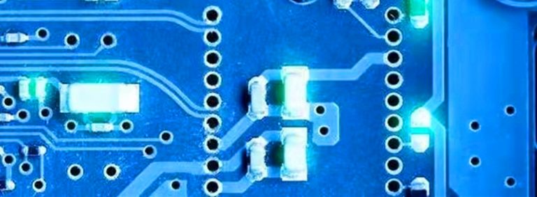
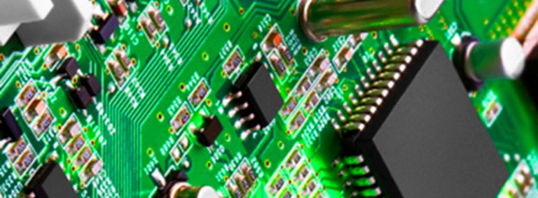
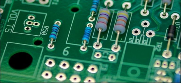
The substrate of the electronic board itself is made of insulating and non-flexible material. The small circuit material that can be seen on the surface is copper foil. The copper foil is originally covered on the entire board, and part of it during the manufacturing process After being etched away, the remaining parts become net-like small circuits. These circuits are called conductor patterns or wiring and are used to provide circuit connections for parts on the PCB.
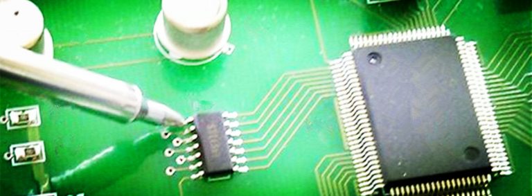
In order to fix the parts on the electronic PCB circuit board, we solder their pins directly on the wiring. On the most basic PCB (single-sided board), the parts are concentrated on one side, and the wires are concentrated on the other side. So It is necessary to make holes in the board so that the pins can pass through the board to the other side, so the pins of the parts are soldered on the other side. Because of this, the front and back sides of the PCB are called the Component Side and Solder Side.
If there are some parts on the custom circuit board that need to be removed or reinstalled after the production is completed, then the socket (Socket) will be used when the part is installed. Since the socket is directly soldered on the board, the parts can be disassembled and assembled at will.

If you want to connect two electronic boards to each other, we generally use edge connectors commonly known as “golden fingers”. The gold fingers contain many exposed copper pads, which are actually part of the PCB wiring. Usually, when connecting, we insert the golden fingers on one PCB into the appropriate slot on the other PCB (generally called the expansion slot Slot). In the computer, such as a graphics card, a sound card, or other similar interface cards, Are connected to the motherboard by golden fingers.
The green or brown on the soldering circuit boards is the color of the solder mask. This layer is an insulating protective layer, which can protect the copper wire and prevent the parts from being soldered to the incorrect place. In addition, the solder mask Will be printed on a layer of silk screen (silkscreen). Usually, text and symbols (mostly white) are printed on this to mark the position of each part on the board. The silkscreen is also called the Icon surface (legend).
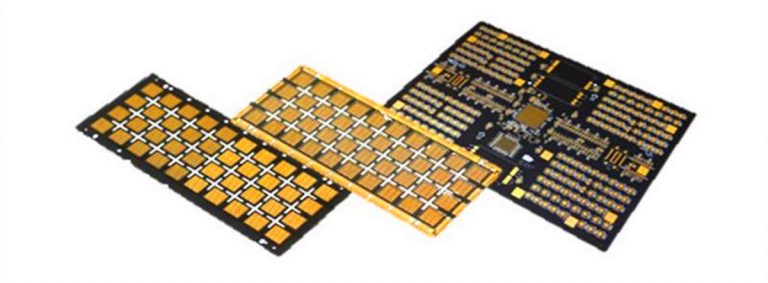
The printed circuit board etches the complex circuit copper wires between parts and parts on a board after careful and neat planning and provides the main support for the installation and interconnection of electronic components. It is indispensable for all electronic products. The basic parts.
The printed circuit board is a flat plate made of non-conductive materials. The flat plate is usually designed with pre-drilled holes to install chips and other electronic components. The hole of the component helps to electronically connect the pre-defined metal paths printed on the board. After the pins of the electronic component are passed through the PCB, the conductive metal welding rod is attached to the PCB to form a circuit.