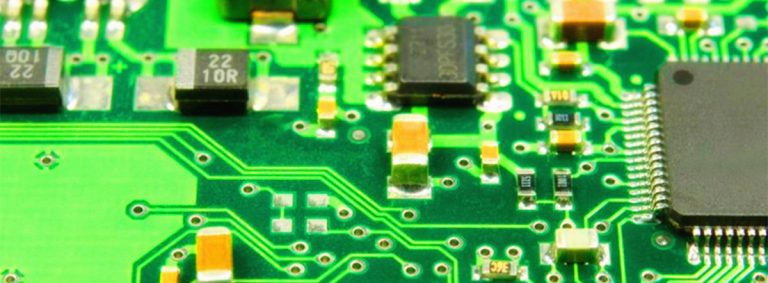

PCB Open Circuit is Encountered by PCB Manufacturers, What is PCB Open Circuit?

PCB open circuit is a problem that PCB manufacturers encounter every day. What is PCB open circuit? In simple terms, a PCB open circuit is two points that should be connected together (point A and point B), but are not connected together.
What is PCB Open Circuit
1. Repeated open circuit
It means that the same open circuit occurs in the same place on the PCB board, which is repeated many times, and the number of the exposure film is the same. The reason for this is that the exposure film is defective at the same position as the open circuit of the board. In this case, the exposure film must be scrapped, and the AOI inspection of the first and last boards during exposure should be strengthened to ensure that the first PCB board is correct. exposure.
2. Gap open circuit
This kind of open circuit is characterized by a gap on a wire, and the remaining line width is less than 1/2 or equal to 1/2 of the normal line width due to the gap. Usually, the position is fixed and repeated many times. The reason for its formation is also because there is a defect on the exposure film, so there is also a gap in the wire at the same position on the PCB. The way to eliminate it is to replace the exposure film with a new one and strengthen the AOI detection during the exposure process.

3. Vacuum open circuit
In a certain area, there are many wires that are getting thinner and thinner (tapering), some form open circuits, some do not, but because the wires are too thin (less than the minimum line width required by the customer) and have to be scrapped . The reason for this defect is that the negative film and the dry film used by the PCB manufacturer are not in close contact with each other, and there is air in the middle, that is, the vacuum is not good after the exposure table is closed, and the vacuum degree cannot meet the requirements, which leads to the change of the wire during exposure. thin or open.
4. Scratch open circuit
Its feature is that the traces of the wires being scratched by external forces can be clearly seen, which also causes an open circuit. The reason is that the wire is scratched due to improper operation (such as the wrong method of holding the board during PCB production, etc.) or the machine to form an open circuit.
Due to the complex causes of outer layer circuit defects, many situations are possible, which are not listed here, but most defects appear on CCL, film, dry film and other materials, or in exposure , development, etching and other processes are abnormal.