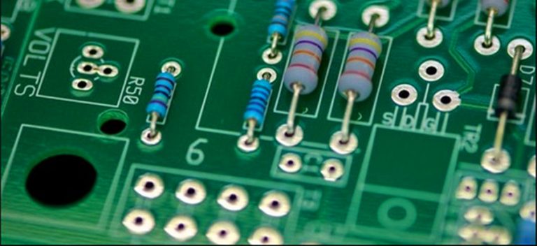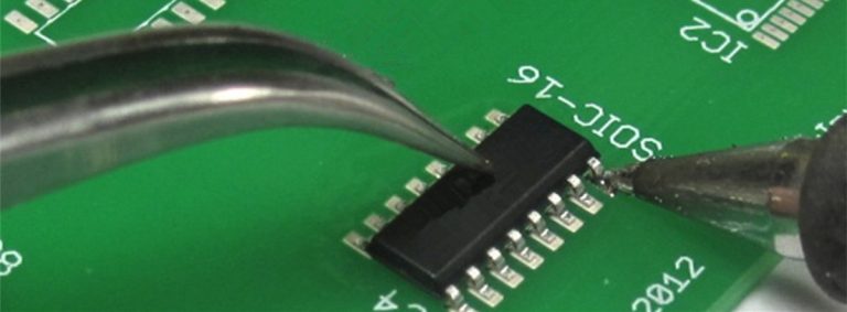
The Causes and Solutions of White Spots in Circuit Board SMT Chip
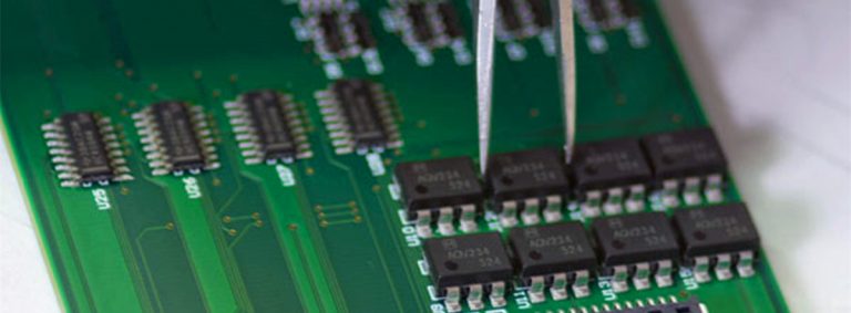
In the SMT patch proofing process of the SMT small-batch patch processing plant, a white spot or white spots in Circuit Board will appear on some circuit boards. What is going on? The appearance inspection also accounts for a large part of the quality inspection of electronic processing. The circuit board with white spots is…